FinFET Vs MOSFET: Energy Efficiency Comparison
SEP 11, 20259 MIN READ
Generate Your Research Report Instantly with AI Agent
Patsnap Eureka helps you evaluate technical feasibility & market potential.
FinFET and MOSFET Evolution and Objectives
The evolution of transistor technology has been a cornerstone of semiconductor advancement since the invention of the Metal-Oxide-Semiconductor Field-Effect Transistor (MOSFET) in the 1960s. This fundamental component has undergone significant transformations to meet the ever-increasing demands for higher performance and lower power consumption in electronic devices. The traditional planar MOSFET dominated the industry for decades, following Moore's Law by consistently shrinking in size while improving performance.
By the early 2000s, as transistor dimensions approached sub-100nm scales, the semiconductor industry faced critical challenges with conventional MOSFET designs. Short-channel effects, gate leakage, and increasing power density emerged as significant barriers to further scaling. These limitations prompted researchers to explore three-dimensional transistor architectures, leading to the development of the Fin Field-Effect Transistor (FinFET) technology.
FinFET represents a revolutionary departure from the planar structure, featuring a thin silicon "fin" that rises vertically from the substrate, with the gate wrapped around three sides of the channel. This multi-gate configuration provides superior electrostatic control over the channel, significantly reducing leakage currents and allowing for continued scaling beyond the limitations of planar MOSFETs.
Intel's introduction of commercial FinFET technology (branded as Tri-Gate) in 2011 at the 22nm node marked a watershed moment in semiconductor manufacturing. This transition demonstrated approximately 37% performance improvement at low voltage and 50% power reduction compared to previous planar transistors, establishing FinFET as the new industry standard for high-performance, energy-efficient computing.
The primary objective of comparing FinFET and MOSFET technologies is to quantify the energy efficiency advantages that three-dimensional architectures offer over traditional planar designs. This analysis aims to provide a comprehensive understanding of how structural differences translate to power consumption benefits across various operating conditions and application scenarios.
Furthermore, this technical exploration seeks to identify the specific mechanisms through which FinFETs achieve superior energy efficiency, including reduced subthreshold leakage, improved short-channel behavior, and enhanced carrier transport properties. Understanding these fundamental advantages is crucial for predicting future scaling trends and evaluating emerging alternatives such as Gate-All-Around (GAA) transistors and nanosheet architectures.
The findings from this comparative analysis will inform strategic decisions regarding technology adoption, process development, and product roadmaps for semiconductor manufacturers and electronic device companies seeking to optimize the power-performance tradeoff in their offerings.
Market Demand for Energy-Efficient Transistors
The global semiconductor market has witnessed a significant shift towards energy-efficient transistor technologies, driven primarily by the exponential growth in mobile devices, data centers, and the Internet of Things (IoT). This market transformation has created substantial demand for advanced transistor architectures that can deliver superior performance while consuming minimal power. The transition from traditional planar MOSFETs to three-dimensional FinFETs represents a critical response to this market need.
Energy efficiency has become a paramount concern across multiple industries. In the mobile sector, consumers increasingly demand longer battery life without compromising device performance. Market research indicates that battery life remains among the top three purchasing considerations for smartphone buyers globally, creating direct pressure on semiconductor manufacturers to develop more efficient transistor technologies.
Data center operators face mounting operational costs related to power consumption and cooling. With global data center electricity consumption reaching approximately 200-250 TWh annually, representing 1% of global electricity demand, the economic incentive for adopting energy-efficient transistor technologies is substantial. Industry analysts estimate that power-related costs can account for over 40% of data center operational expenses.
The automotive industry presents another rapidly expanding market for energy-efficient transistors. As electric vehicles gain market share, the demand for semiconductor components that maximize battery efficiency continues to grow. The automotive semiconductor market specifically for power-efficient components is expanding at a compound annual growth rate exceeding 10%.
Environmental regulations and corporate sustainability initiatives further accelerate market demand for energy-efficient transistor technologies. Many jurisdictions have implemented energy efficiency standards that effectively mandate the adoption of advanced semiconductor technologies in consumer electronics and industrial equipment.
From a competitive standpoint, semiconductor manufacturers who can deliver superior energy efficiency gain significant market advantages. This has intensified research and development investments in FinFET technology, with major foundries allocating billions to advance their manufacturing capabilities. The market premium for chips offering better performance-per-watt metrics demonstrates the economic value placed on energy efficiency.
The IoT market segment presents perhaps the most stringent energy requirements, with many applications demanding ultra-low power consumption for battery-powered or energy-harvesting devices. This has created a specialized market niche for transistor technologies optimized for near-threshold or sub-threshold operation, where the efficiency advantages of FinFETs over traditional MOSFETs become particularly pronounced.
Technical Challenges in Transistor Energy Efficiency
The energy efficiency of transistors has become a critical bottleneck in semiconductor advancement, with both FinFET and traditional MOSFET architectures presenting unique challenges. The planar MOSFET design faces severe limitations as dimensions shrink below 22nm, particularly with short-channel effects causing increased leakage current and static power consumption. These effects manifest as drain-induced barrier lowering (DIBL), threshold voltage roll-off, and subthreshold swing degradation, all contributing to exponentially increasing power density.
FinFET technology, while offering superior electrostatic control through its three-dimensional gate structure, introduces new manufacturing complexities. The fin formation process requires precise etching techniques to maintain uniform fin dimensions, as variations can lead to significant threshold voltage fluctuations across the chip. Additionally, the increased surface area of the fin structure creates higher parasitic capacitance, affecting switching speed and dynamic power consumption during high-frequency operations.
Heat dissipation represents another major challenge in both architectures but manifests differently. In planar MOSFETs, the two-dimensional heat flow pattern creates hotspots that are difficult to manage as device density increases. FinFETs, with their three-dimensional structure, present more complex thermal pathways that complicate cooling solutions, particularly in stacked configurations where heat from lower layers must traverse through multiple device layers.
The gate oxide scaling presents a fundamental physical limitation for both technologies. As oxide thickness approaches atomic dimensions (below 1nm), quantum tunneling effects dramatically increase gate leakage current. While high-k dielectric materials have partially addressed this issue, the interface quality between these materials and the channel remains problematic, creating charge trapping sites that degrade carrier mobility and reliability.
Source/drain resistance has emerged as a dominant factor limiting energy efficiency in advanced nodes. As channel lengths decrease, the relative contribution of contact resistance to total device resistance increases substantially. This parasitic resistance not only reduces drive current but also increases power dissipation during switching operations, creating a fundamental energy efficiency challenge that affects both architectures but becomes particularly acute in FinFETs due to their complex geometry.
Multi-gate control in FinFETs, while beneficial for electrostatic integrity, introduces synchronization challenges between gates that can lead to increased switching energy if not properly managed. The process variations in fin width and height further exacerbate this issue, creating inconsistent threshold voltages that necessitate higher operating voltages to ensure reliable operation across all transistors, thereby reducing overall energy efficiency.
Current Energy Efficiency Solutions
01 FinFET structure advantages over traditional MOSFET
FinFET transistors offer significant energy efficiency improvements over traditional planar MOSFETs due to their three-dimensional structure. The fin-shaped channel allows for better electrostatic control of the gate over the channel, reducing leakage current and improving power consumption. This architecture enables operation at lower threshold voltages while maintaining performance, resulting in reduced dynamic power consumption in integrated circuits.- FinFET structure advantages over traditional MOSFET: FinFET transistors offer significant energy efficiency improvements over traditional planar MOSFETs due to their three-dimensional structure. The fin-shaped channel allows for better electrostatic control of the gate over the channel, reducing leakage current and improving power consumption. This architecture enables operation at lower threshold voltages while maintaining performance, resulting in reduced dynamic power consumption in integrated circuits.
- Multi-gate configurations for power optimization: Multi-gate configurations in FinFET designs provide enhanced control over channel current and significantly improve energy efficiency. By surrounding the channel with gate material on multiple sides, these configurations reduce short-channel effects and allow for better scaling. The improved gate control enables lower operating voltages and reduced power consumption while maintaining performance characteristics, making them ideal for energy-efficient applications.
- Advanced power management techniques: Various power management techniques have been developed specifically for FinFET and MOSFET technologies to optimize energy efficiency. These include dynamic voltage and frequency scaling, power gating, and adaptive body biasing. Implementation of these techniques allows for significant reduction in both static and dynamic power consumption, enabling more energy-efficient operation in various application scenarios from mobile devices to data centers.
- Process technology optimization for energy efficiency: Advanced process technologies specifically optimized for FinFET manufacturing have been developed to enhance energy efficiency. These include specialized doping profiles, strain engineering techniques, and high-k metal gate integration. These process optimizations reduce parasitic capacitances and resistances, leading to faster switching speeds at lower power consumption levels, thereby improving the overall energy efficiency of FinFET-based integrated circuits.
- Circuit design techniques for FinFET energy optimization: Specialized circuit design techniques have been developed to leverage the unique characteristics of FinFET technology for maximum energy efficiency. These include FinFET-specific standard cell libraries, memory designs, and I/O circuits that take advantage of the superior electrostatic properties of FinFETs. By optimizing circuit topologies and sizing specifically for FinFET technology, significant improvements in energy efficiency can be achieved compared to traditional MOSFET-based designs.
02 Multi-gate technology for power optimization
Multi-gate technology employed in FinFETs provides enhanced control over the channel, allowing for better power management. By surrounding the channel with gates on multiple sides, these transistors can operate at lower voltages while maintaining performance. This configuration reduces short-channel effects and improves subthreshold swing, leading to significant power savings in high-performance computing applications and mobile devices.Expand Specific Solutions03 Scaling benefits for energy efficiency
The superior scaling capabilities of FinFETs contribute to their energy efficiency advantages. As transistor dimensions shrink, FinFETs maintain better performance characteristics than planar MOSFETs, particularly at advanced technology nodes. The vertical fin structure allows for effective channel length control even at smaller dimensions, enabling continued voltage scaling and power reduction while maintaining performance metrics and mitigating short-channel effects.Expand Specific Solutions04 Circuit design optimization for FinFET technology
Circuit design techniques specifically optimized for FinFET technology can further enhance energy efficiency. These include adaptive voltage scaling, power gating, and clock gating methodologies tailored to the unique characteristics of FinFET devices. By leveraging the inherent advantages of FinFET structures in circuit design, significant power savings can be achieved in various applications including processors, memory, and mixed-signal circuits.Expand Specific Solutions05 Manufacturing process innovations for energy-efficient transistors
Advanced manufacturing processes for FinFETs contribute to their energy efficiency advantages. Innovations in materials, such as high-k gate dielectrics and metal gates, combined with precise fin formation techniques, enable the production of transistors with optimized performance and power characteristics. These process improvements reduce parasitic capacitances and resistances, leading to faster switching speeds at lower power consumption compared to conventional MOSFET technologies.Expand Specific Solutions
Leading Semiconductor Manufacturers Analysis
The FinFET vs MOSFET energy efficiency comparison represents a critical technological evolution in semiconductor manufacturing, currently in a mature growth phase with increasing market adoption. The global market is substantial, driven by demand for energy-efficient computing solutions from key players like TSMC, Samsung, and Intel. Technologically, FinFET has achieved significant maturity with companies like GlobalFoundries, TSMC, and IBM demonstrating advanced implementations that deliver superior power efficiency compared to traditional planar MOSFETs. Samsung and Intel have further refined multi-gate architectures, while AMD and Infineon leverage these technologies in their product designs. The competitive landscape continues to evolve as manufacturers balance performance gains against manufacturing complexity.
Taiwan Semiconductor Manufacturing Co., Ltd.
Technical Solution: TSMC has pioneered advanced FinFET technology since its 16nm node introduction, evolving through 10nm, 7nm, 5nm, and now 3nm processes. Their FinFET architecture employs a three-dimensional transistor structure where the gate wraps around three sides of the elevated channel (fin), significantly reducing leakage current compared to planar MOSFETs. TSMC's latest FinFET technologies incorporate strain engineering, high-mobility channel materials, and advanced gate stacks to enhance carrier mobility and reduce operating voltage[1]. Their N3 (3nm) FinFET technology achieves approximately 70% logic density gain, up to 15% speed improvement at the same power, and up to 30% power reduction at the same speed compared to their N5 process[2]. TSMC has also developed multi-bridge channel FET (MBCFET) technology as an evolution of FinFET for future nodes, further improving electrostatic control and energy efficiency.
Strengths: Superior electrostatic control leading to significantly reduced leakage current; higher drive current capability at the same leakage; ability to operate at lower voltages; better short-channel effect control. Weaknesses: More complex manufacturing process requiring additional lithography steps; higher production costs; increased parasitic capacitance; challenges in heat dissipation due to 3D structure.
Semiconductor Manufacturing International (Shanghai) Corp.
Technical Solution: SMIC has developed FinFET technology focusing on the 14nm node and beyond, representing China's most advanced semiconductor manufacturing capability. Their FinFET implementation features optimized fin geometry with height-to-width ratios designed for balanced performance and power efficiency. SMIC's 14nm FinFET process demonstrates approximately 20% higher performance or 60% lower power consumption compared to their 28nm planar MOSFET technology[9]. The company has implemented specialized strain engineering techniques including the use of embedded SiGe source/drain regions for p-channel devices to enhance carrier mobility. SMIC's FinFET technology incorporates high-k metal gate (HKMG) materials with carefully tuned work functions to optimize threshold voltages for different application requirements. Their designs show particular advantages in mobile and IoT applications, where their FinFET technology enables significant battery life improvements while maintaining performance targets. SMIC has also developed specialized low-power variants of their FinFET technology that can operate at near-threshold voltages, further improving energy efficiency for specific applications[10].
Strengths: Cost-competitive manufacturing; good power efficiency for mobile applications; balanced performance characteristics; growing ecosystem support within China. Weaknesses: Less mature technology compared to global leaders; higher variability in certain performance parameters; limited to less advanced nodes compared to TSMC and Samsung; challenges in achieving consistent yields at scale.
Key Innovations in FinFET Technology
Ultra low power 16-bit arithmatic logic unit
PatentPendingIN202031039065A
Innovation
- The integration of FinFET technology with adiabatic logic principles, specifically using trapezoidal or sinusoidal waveforms for clocking, allows for energy recycling and reduced power consumption by optimizing switching time and energy return to the power source, resulting in a novel 16-Bit Arithmetic Logic Unit (ALU) architecture.
Semiconductor device and the method of manufacturing the same
PatentActiveUS20200075594A1
Innovation
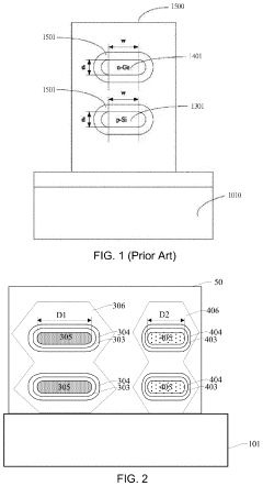
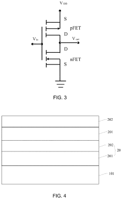
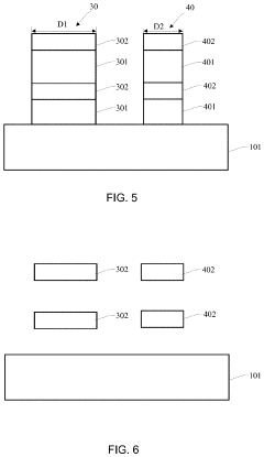
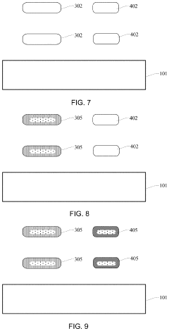
- A three-dimensional stacked gate-all-around nanosheet complementary inverter with junctionless transistors and a gradient channel doping profile is introduced, featuring P-type and N-type semiconductor channels with varying doping concentrations and cross-sectional widths, along with specific materials and manufacturing methods to enhance mobility and reduce resistance.
Thermal Management Strategies
Thermal management represents a critical factor in the energy efficiency comparison between FinFET and MOSFET technologies. As transistor densities increase and dimensions shrink, heat dissipation has become a primary concern affecting both performance and power consumption. The three-dimensional structure of FinFETs introduces unique thermal challenges compared to planar MOSFETs, necessitating specialized management strategies.
For traditional planar MOSFETs, thermal management typically relies on conventional heat spreading techniques through the substrate. These include backside cooling methods, thermal interface materials (TIMs), and heat sinks. However, as device scaling continues, these approaches have proven increasingly insufficient, particularly in high-performance applications where thermal throttling limits operational efficiency.
FinFET architectures, with their vertical fin structures, present both challenges and opportunities for thermal management. The reduced contact area between the channel and substrate restricts heat flow paths, potentially leading to localized hotspots. Research indicates that FinFETs can experience temperature increases 15-20% higher than planar devices under similar operating conditions, directly impacting leakage current and reliability.
Advanced cooling solutions specifically designed for FinFET technologies include microchannel liquid cooling systems that can be integrated closer to the heat source. These systems have demonstrated the ability to reduce junction temperatures by up to 30°C compared to conventional air cooling, significantly improving energy efficiency by reducing leakage power. Additionally, phase-change materials (PCMs) embedded within the packaging provide thermal buffering during transient workloads, preventing thermal spikes that would otherwise trigger dynamic voltage and frequency scaling.
Thermal-aware circuit design has emerged as a crucial strategy for both technologies. For FinFETs, this includes optimized fin spacing and orientation to enhance heat dissipation while maintaining electrical performance. Computational fluid dynamics (CFD) modeling has become essential in predicting thermal behavior and optimizing physical layouts before fabrication, reducing design iterations and associated costs.
Recent innovations in thermally conductive materials show particular promise for FinFET implementations. Diamond-based heat spreaders with thermal conductivity exceeding 1500 W/mK (compared to silicon's 150 W/mK) have demonstrated the ability to reduce peak temperatures by up to 40% in high-performance FinFET designs. Similarly, graphene-based thermal interface materials are being explored to enhance heat transfer across packaging boundaries.
The energy efficiency advantage of FinFETs over MOSFETs is significantly influenced by these thermal management strategies. When properly implemented, advanced thermal solutions can help FinFETs maintain their theoretical efficiency advantages even under sustained high-performance workloads, where traditional MOSFETs would experience greater performance degradation due to thermal limitations.
Scaling Limitations and Beyond-FinFET Technologies
As semiconductor technology continues to advance, traditional planar MOSFET scaling faces fundamental physical limitations. The 20nm node represents a critical threshold where conventional scaling encounters severe short-channel effects, increased leakage currents, and diminished electrostatic control. These challenges have necessitated the transition to three-dimensional architectures like FinFET, which has successfully extended Moore's Law through superior channel control and reduced leakage.
However, FinFET technology itself is approaching scaling limits. At nodes below 5nm, fin width control becomes increasingly difficult, quantum confinement effects become more pronounced, and parasitic capacitance issues intensify. The fin geometry presents fabrication challenges at extreme dimensions, limiting the potential for further miniaturization while maintaining performance advantages.
Industry and research institutions are actively exploring several promising beyond-FinFET technologies. Gate-all-around (GAA) FETs, particularly nanosheet and nanowire transistors, offer enhanced electrostatic control by surrounding the channel with gate material on all sides. These structures demonstrate superior subthreshold characteristics and reduced short-channel effects compared to FinFETs, making them strong candidates for 3nm nodes and beyond.
Complementary FET (CFET) technology, which stacks n-type and p-type transistors vertically rather than placing them side by side, represents another innovative approach. This configuration significantly reduces the transistor footprint, enabling higher integration density while potentially improving power efficiency through reduced interconnect lengths.
2D material-based transistors utilizing materials like graphene, molybdenum disulfide, and other transition metal dichalcogenides offer atomically thin channels with excellent carrier mobility. These materials could potentially enable sub-nanometer scaling while addressing quantum tunneling issues that plague silicon at extreme dimensions.
Tunnel FETs (TFETs) represent a more radical departure from conventional MOSFET operation, utilizing band-to-band tunneling instead of thermionic emission. This approach potentially allows for sub-60mV/decade subthreshold swing, enabling significant power reduction at low operating voltages, though challenges remain in achieving sufficient ON-state current.
The transition beyond FinFET will likely involve hybrid approaches initially, combining aspects of multiple technologies to balance performance, power efficiency, and manufacturability before any single solution emerges as dominant in the semiconductor roadmap.
Unlock deeper insights with Patsnap Eureka Quick Research — get a full tech report to explore trends and direct your research. Try now!
Generate Your Research Report Instantly with AI Agent
Supercharge your innovation with Patsnap Eureka AI Agent Platform!
