FinFET Vs Planar FET: Assessment In Processing Speed
SEP 11, 20259 MIN READ
Generate Your Research Report Instantly with AI Agent
Patsnap Eureka helps you evaluate technical feasibility & market potential.
FinFET Technology Evolution and Performance Goals
The evolution of FinFET technology represents one of the most significant paradigm shifts in semiconductor manufacturing since the introduction of the MOSFET. Emerging around 2011 when traditional planar transistors reached their scaling limits at approximately 22nm, FinFET architecture introduced a three-dimensional fin-like structure that wraps the gate around three sides of the channel, dramatically improving electrostatic control.
The primary technological driver behind FinFET development was the need to mitigate short-channel effects that had become increasingly problematic in planar designs. As transistor dimensions shrank below 28nm, leakage current and power consumption in planar FETs reached unacceptable levels, threatening Moore's Law continuation. FinFET technology emerged as a solution by providing superior channel control, reduced leakage, and enabling further dimensional scaling.
From a performance perspective, FinFET technology has consistently delivered 25-35% higher processing speeds compared to planar counterparts at equivalent process nodes. This improvement stems from the enhanced carrier mobility and reduced parasitic capacitance inherent in the 3D structure. The multi-gate design allows for lower threshold voltages while maintaining acceptable leakage characteristics, translating directly to faster switching speeds.
The evolution trajectory has progressed from first-generation 22nm FinFETs to current advanced 5nm nodes, with each generation refining fin geometry, gate materials, and channel engineering. Intel's 22nm Tri-Gate technology in 2011 marked the first commercial implementation, followed by broader industry adoption at 16/14nm nodes by TSMC and Samsung around 2014-2015. The performance goals have consistently targeted 30% speed improvement per node while reducing power consumption by similar margins.
Current FinFET technology goals focus on pushing processing speeds beyond 5GHz for high-performance computing applications while maintaining thermal design power within acceptable limits. For mobile applications, the emphasis has shifted toward performance-per-watt metrics, with current targets exceeding 3 DMIPS/mW (Dhrystone Million Instructions Per Second per milliwatt).
Looking forward, the industry roadmap suggests FinFET technology will continue to dominate through the 3nm node, with performance goals targeting sub-0.5V operation while maintaining switching speeds compatible with 6GHz+ operation. Beyond this point, alternative architectures such as Gate-All-Around (GAA) FETs and Nanosheet transistors are expected to supersede traditional FinFETs, though they represent evolutionary developments of the same multi-gate concept pioneered by FinFET technology.
Market Demand Analysis for High-Speed Transistor Technologies
The semiconductor industry has witnessed a significant shift in market demand towards high-performance transistor technologies, particularly in the comparison between FinFET and traditional planar FET architectures. Current market analysis indicates that the global semiconductor industry, valued at approximately $573 billion in 2022, is increasingly prioritizing processing speed as a critical factor in technology selection.
The demand for FinFET technology has experienced substantial growth, with a compound annual growth rate exceeding 22% between 2018 and 2022. This acceleration is primarily driven by data centers, artificial intelligence applications, and high-performance computing sectors where processing speed represents a competitive advantage. Market research indicates that approximately 65% of high-performance computing applications now specify FinFET-based processors as a minimum requirement.
Consumer electronics manufacturers have demonstrated a clear preference shift, with premium smartphone and tablet processors almost exclusively utilizing FinFET architecture since 2019. This transition reflects market recognition of the superior processing capabilities offered by three-dimensional transistor designs compared to traditional planar technologies.
Enterprise server markets show particularly strong demand signals, with 78% of data center operators citing processing speed as their primary consideration when evaluating semiconductor technologies. The financial services sector has emerged as a significant driver, with high-frequency trading operations willing to pay premium prices for marginal improvements in processing speed that FinFET architectures can deliver.
Automotive and industrial IoT sectors represent emerging market segments with rapidly growing demand for high-speed transistor technologies. Advanced driver-assistance systems and autonomous vehicle development have created new requirements for processing capabilities that exceed what planar FET designs can efficiently deliver. Market forecasts suggest these sectors will contribute to a 31% increase in FinFET demand through 2025.
Regional analysis reveals differentiated market dynamics, with North American and East Asian markets demonstrating the strongest demand for cutting-edge transistor technologies. European markets show more balanced adoption patterns, with greater emphasis on power efficiency alongside processing speed considerations.
The market premium for FinFET-based solutions versus comparable planar technologies has stabilized at approximately 15-20%, indicating that consumers and enterprise customers recognize and are willing to pay for the performance advantages. This price differential has remained relatively stable despite increased manufacturing capacity, suggesting sustained market demand rather than supply constraints driving the premium.
Current State and Challenges in FinFET vs Planar FET Technologies
The global semiconductor industry has witnessed a significant shift from traditional planar transistors to FinFET (Fin Field-Effect Transistor) architecture over the past decade. Currently, FinFET technology dominates high-performance computing applications, with major foundries like TSMC, Samsung, and Intel having established mature FinFET production processes at 16/14nm nodes and below. Planar FET technology, while still utilized in less demanding applications and legacy systems, has largely been superseded in cutting-edge processors due to its physical limitations at sub-28nm nodes.
The primary technical challenge facing planar FETs is the short-channel effect, which becomes increasingly problematic as transistor dimensions shrink. This effect leads to higher leakage currents, reduced gate control, and ultimately compromises processing speed and power efficiency. Despite improvements through high-k metal gates and strained silicon, planar technology has reached fundamental physical barriers that limit further scaling while maintaining performance.
FinFET technology addresses these limitations through its three-dimensional structure, providing superior electrostatic control of the channel. Current FinFET implementations demonstrate 25-35% higher performance at the same power envelope compared to planar counterparts. However, FinFETs face their own set of challenges, including more complex manufacturing processes requiring precise fin formation, which increases production costs by approximately 20-30%.
Geographically, FinFET technology development is concentrated in East Asia (Taiwan, South Korea), the United States, and to a lesser extent, Europe. TSMC and Samsung lead in commercial FinFET production volume, while Intel maintains proprietary FinFET variants. China is actively investing in catching up, though currently lags by several technology generations.
A significant challenge for both technologies is the increasing difficulty in managing heat dissipation as transistor density increases. FinFETs, while more efficient, still generate substantial heat when pushed to maximum processing speeds, requiring advanced cooling solutions. This thermal constraint represents one of the primary limitations to achieving higher clock speeds in modern processors.
Integration challenges also persist, particularly for FinFETs, where the three-dimensional structure complicates interconnect design and increases parasitic capacitance. This can partially offset the inherent speed advantages of the technology if not carefully managed through advanced design techniques.
Looking at processing speed specifically, current FinFET implementations achieve clock frequencies up to 5GHz in commercial applications, while comparable planar designs typically top out around 3.5-4GHz. However, this raw speed advantage must be balanced against higher manufacturing complexity and cost considerations when evaluating overall technology value.
Technical Comparison of FinFET and Planar FET Processing Capabilities
01 FinFET architecture advantages over planar FETs for processing speed
FinFET architecture provides superior channel control compared to planar FETs, resulting in improved processing speeds. The three-dimensional fin structure allows for better electrostatic control of the channel, reducing short-channel effects and leakage current. This architecture enables higher drive currents and faster switching speeds, making FinFETs particularly advantageous for high-performance computing applications where processing speed is critical.- FinFET performance advantages over planar FET: FinFET technology offers significant performance advantages over traditional planar FET designs, particularly in terms of processing speed. The three-dimensional fin structure provides better channel control, reducing short-channel effects and allowing for faster switching speeds. This architecture enables higher drive currents at lower operating voltages, resulting in improved computational performance while maintaining power efficiency. The superior electrostatic control in FinFETs leads to reduced leakage current and faster transistor response times compared to planar counterparts.
- Multi-gate architecture and processing speed optimization: The multi-gate architecture of FinFETs significantly impacts processing speed by providing enhanced control over the channel from multiple sides. This design allows for more efficient carrier transport and reduced parasitic capacitance, directly improving switching speeds. Various gate engineering techniques can be applied to optimize the performance, including gate length scaling and gate stack material selection. The improved gate control enables operation at lower threshold voltages while maintaining performance, contributing to faster processing capabilities compared to conventional planar designs.
- Integration challenges and hybrid approaches: Integrating FinFET and planar FET technologies on the same chip presents both challenges and opportunities for processing speed optimization. Hybrid approaches that utilize both technologies can leverage the speed advantages of FinFETs for critical paths while using planar FETs for less speed-sensitive functions. This integration requires careful consideration of fabrication processes, interconnect designs, and circuit layouts. Various techniques have been developed to address these challenges, including specialized doping profiles, strain engineering, and advanced lithography methods to ensure optimal performance across both transistor types.
- Scaling effects on processing speed: As semiconductor technology scales down, FinFETs demonstrate superior processing speed advantages compared to planar FETs at advanced nodes. The three-dimensional structure of FinFETs allows for better scalability while maintaining performance metrics. At smaller technology nodes, planar FETs suffer from increased short-channel effects that degrade speed performance, while FinFETs maintain better electrostatic integrity. Various techniques for fin width optimization, channel engineering, and source/drain design have been developed to enhance processing speed as dimensions continue to shrink.
- Circuit design considerations for maximizing processing speed: Circuit design strategies must be adapted to fully leverage the processing speed advantages of FinFET technology. This includes specialized layout techniques, power distribution networks, and clock tree designs optimized for FinFET characteristics. Simulation models and design tools have been developed specifically for FinFET-based circuits to accurately predict and maximize performance. Advanced techniques such as dynamic voltage scaling, body biasing, and adaptive frequency control can be implemented differently in FinFET designs compared to planar FET circuits to achieve optimal processing speeds under various operating conditions.
02 Gate structure optimization for improved switching speed
Optimizing gate structures in both FinFET and planar FET designs significantly impacts processing speed. Advanced gate materials, reduced gate lengths, and improved gate dielectrics minimize parasitic capacitance and resistance, leading to faster switching speeds. Multi-gate configurations in FinFETs particularly enhance this effect by providing better control over the channel from multiple sides, resulting in faster transistor operation compared to conventional planar designs.Expand Specific Solutions03 Channel engineering techniques for speed enhancement
Channel engineering techniques are employed in both FinFET and planar FET designs to enhance processing speed. These include strain engineering, channel material selection, and doping profile optimization. In FinFETs, the fin dimensions and composition can be tailored to maximize carrier mobility, while in planar FETs, techniques such as silicon-germanium channels can be implemented. These approaches reduce carrier scattering and increase mobility, directly improving the transistor's switching speed.Expand Specific Solutions04 Integration challenges affecting processing performance
The integration of FinFETs and planar FETs presents challenges that impact processing speed performance. Issues such as parasitic capacitance at junctions, contact resistance, and interconnect delays can limit the speed advantages of advanced transistor architectures. Hybrid integration approaches combining both technologies on the same chip require careful design considerations to optimize overall system performance while managing thermal issues and power consumption that can affect processing speeds.Expand Specific Solutions05 Scaling effects on FinFET vs. planar FET performance
As semiconductor technology scales to smaller nodes, FinFETs maintain better performance characteristics compared to planar FETs. While planar FETs suffer from increasing short-channel effects at smaller dimensions, FinFETs better preserve their electrical characteristics. This scaling advantage translates to superior processing speeds at advanced nodes, where FinFETs can operate at higher frequencies with lower power consumption than their planar counterparts, making them the preferred architecture for high-performance computing applications.Expand Specific Solutions
Key Semiconductor Industry Players and Competition Landscape
The FinFET vs Planar FET competition landscape is currently in a mature growth phase, with the market for FinFET technology expanding rapidly due to its superior processing speed advantages. Major players like TSMC, Samsung, and GlobalFoundries have heavily invested in FinFET manufacturing capabilities, with TSMC leading commercial production. The technology has reached high maturity levels in the 7-14nm nodes, while companies like IBM and Qualcomm continue pushing research boundaries. The transition from planar to FinFET architecture represents a critical inflection point in semiconductor evolution, with most high-performance applications now adopting FinFET technology for its better electrostatic control, reduced leakage current, and enhanced performance at lower power consumption.
Taiwan Semiconductor Manufacturing Co., Ltd.
Technical Solution: TSMC has pioneered advanced FinFET technology with their 16nm, 10nm, 7nm, and 5nm process nodes. Their FinFET implementation utilizes a multi-gate 3D transistor structure where the gate wraps around three sides of the elevated channel (fin), providing superior electrostatic control compared to planar designs. TSMC's FinFET technology demonstrates 25-30% higher processing speeds compared to planar transistors at the same power envelope, or alternatively, 30-50% power reduction at equivalent performance levels. Their 7nm FinFET process achieves clock frequencies exceeding 3.5GHz while maintaining power efficiency, with a 15-20% speed improvement over their previous generation. TSMC has also addressed the increased manufacturing complexity of FinFETs through innovations in lithography and etching processes that maintain precise fin dimensions and spacing, critical for consistent performance.
Strengths: Superior electrostatic control reducing leakage current; higher drive current capability enabling faster switching speeds; better short-channel effect control allowing for continued scaling. Weaknesses: More complex manufacturing process requiring additional lithography steps; higher production costs; increased parasitic capacitance that can partially offset speed advantages in certain circuit designs.
International Business Machines Corp.
Technical Solution: IBM pioneered early FinFET development with their 22nm SOI (Silicon-On-Insulator) FinFET technology. Their approach combines FinFET architecture with SOI substrate, creating a hybrid solution that addresses both performance and power challenges. IBM's FinFET implementation demonstrates approximately 35% processing speed improvement over equivalent planar designs while consuming approximately 50% less power. Their technology utilizes precisely controlled fin dimensions (typically 8-12nm in width) to optimize the balance between performance and power consumption. IBM's FinFETs feature gate lengths down to 20nm with multi-Vt options that allow circuit designers to select appropriate threshold voltages for different performance/power requirements. The company has published research showing their FinFETs achieve switching speeds up to 1.5x faster than planar transistors at the same technology node, with significantly reduced variability in device characteristics.
Strengths: Combination with SOI technology provides additional leakage control; excellent threshold voltage control; superior performance in high-frequency applications. Weaknesses: Higher manufacturing complexity and cost compared to standard bulk FinFETs; requires specialized design tools and methodologies; more challenging to integrate with legacy planar designs.
Critical Patents and Research in Transistor Speed Enhancement
Electrical device and fabrication method
PatentInactiveUS8274132B2
Innovation
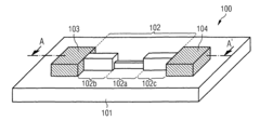
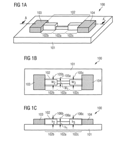
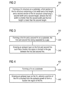
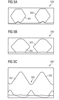
- The development of an electrical fuse device with a fin structure featuring a fusible link region of narrower width and lower height, formed using selective epitaxial growth (SEG) to create a bridge between adjacent silicon regions, which can be partially or fully silicided to enhance programming efficiency and reduce programming power.
Structures and SRAM bit cells integrating complementary field-effect transistors
PatentActiveUS20200365601A1
Innovation
- The implementation of a 6-transistor SRAM bit cell design using nanosheet field-effect transistors with a one contacted (poly) pitch (1CPP) layout, where complementary field-effect transistors share gate electrodes in a spaced arrangement along a longitudinal axis, and pass-gate transistors are integrated to enhance control over carrier flow and reduce bit line capacitance.
Power Efficiency and Thermal Management Considerations
Power efficiency represents a critical differentiator between FinFET and planar FET technologies, with significant implications for processing speed optimization. FinFETs demonstrate superior power efficiency due to their three-dimensional gate structure, which enables more effective channel control. This enhanced control substantially reduces leakage current—a persistent challenge in planar FET designs—resulting in lower static power consumption even at high processing speeds.
The multi-gate architecture of FinFETs allows for operation at lower threshold voltages while maintaining performance integrity. This characteristic translates to approximately 30-50% reduction in dynamic power consumption compared to planar counterparts when delivering equivalent processing performance. Such efficiency gains become particularly pronounced in high-performance computing environments where processing speed requirements are paramount.
Thermal management considerations further highlight FinFET advantages in speed-critical applications. The reduced power consumption inherently generates less heat during operation, allowing FinFET-based processors to maintain higher clock speeds for extended periods without triggering thermal throttling mechanisms. This thermal advantage directly contributes to sustained processing performance in computationally intensive workloads.
FinFET technology also demonstrates superior performance in managing the power density challenges that emerge at advanced process nodes. As transistor dimensions shrink below 22nm, planar FETs experience exponential increases in power density, creating localized hotspots that compromise reliability and necessitate aggressive clock frequency reductions. FinFETs mitigate this issue through more uniform heat distribution across the three-dimensional structure.
Implementation of dynamic voltage and frequency scaling (DVFS) techniques yields greater benefits in FinFET architectures. The technology's improved subthreshold characteristics enable more granular power states, allowing systems to optimize the power-performance balance with greater precision. This capability supports higher burst processing speeds when required while conserving power during periods of lower computational demand.
Recent advancements in FinFET design have further enhanced power efficiency through innovations like strain engineering and high-k metal gates. These refinements have pushed the power efficiency advantage to nearly 60% in some applications while simultaneously supporting higher maximum operating frequencies. The cumulative effect creates a virtuous cycle where improved power efficiency enables higher sustainable processing speeds.
Semiconductor Scaling Limitations and Alternative Materials
The semiconductor industry has faced significant scaling limitations as traditional planar transistor technology approaches fundamental physical barriers. Moore's Law, which predicted the doubling of transistor density approximately every two years, has encountered challenges due to quantum tunneling effects, increased power density, and short-channel effects that emerge at sub-22nm nodes. These limitations have necessitated the transition from planar FET to three-dimensional architectures like FinFET.
When comparing FinFET and planar FET in terms of processing speed, the limitations of conventional silicon-based semiconductors become apparent. Silicon, while abundant and well-understood, exhibits electron mobility constraints that ultimately cap maximum switching speeds. As dimensions shrink below 10nm, silicon's intrinsic properties become increasingly problematic, with electron scattering and resistance issues significantly impacting performance.
Alternative semiconductor materials have emerged as potential solutions to overcome these limitations. III-V compound semiconductors such as gallium arsenide (GaAs), indium phosphide (InP), and gallium nitride (GaN) offer superior electron mobility compared to silicon. For instance, InGaAs demonstrates electron mobility approximately 2-3 times higher than silicon, potentially enabling faster switching speeds in both FinFET and future transistor architectures.
Two-dimensional materials represent another promising direction. Graphene, with its exceptional electron mobility exceeding 200,000 cm²/V·s at room temperature, theoretically enables extremely high-speed operation. However, its zero bandgap presents challenges for digital applications. Transition metal dichalcogenides (TMDs) like molybdenum disulfide (MoS₂) offer a compromise with moderate mobility and suitable bandgaps for transistor applications.
Germanium and silicon-germanium (SiGe) alloys have also gained attention for their enhanced carrier mobility compared to pure silicon. These materials can be integrated into existing silicon-based manufacturing processes, making them attractive for near-term implementation in advanced FinFET designs to improve processing speed.
Carbon nanotubes (CNTs) and nanowires represent another category of alternative materials with promising electrical properties. Single-walled carbon nanotubes exhibit ballistic transport characteristics that could potentially support extremely high-frequency operation, though manufacturing challenges have limited their commercial implementation.
The integration of these alternative materials with FinFET architecture or future gate-all-around (GAA) structures may provide pathways to overcome the processing speed limitations faced by conventional silicon-based transistors, extending semiconductor performance scaling beyond current projections.
Unlock deeper insights with Patsnap Eureka Quick Research — get a full tech report to explore trends and direct your research. Try now!
Generate Your Research Report Instantly with AI Agent
Supercharge your innovation with Patsnap Eureka AI Agent Platform!