

Gate Resistance Optimization For SiC MOSFET Switching
SEP 8, 20259 MIN READ
Generate Your Research Report Instantly with AI Agent
PatSnap Eureka helps you evaluate technical feasibility & market potential.
SiC MOSFET Gate Resistance Background and Objectives
Silicon Carbide (SiC) MOSFET technology has emerged as a revolutionary advancement in power electronics over the past two decades. The evolution of this wide bandgap semiconductor material has fundamentally transformed high-power switching applications by offering superior performance characteristics compared to traditional silicon-based devices. SiC MOSFETs provide higher breakdown voltage, faster switching speeds, lower on-resistance, and better thermal conductivity, enabling more efficient power conversion systems across various industries.
The gate resistance parameter in SiC MOSFETs represents a critical design consideration that significantly impacts switching performance. Historically, power electronics engineers have faced a fundamental trade-off: lower gate resistance values enable faster switching transitions and reduced switching losses, while higher resistance values help mitigate electromagnetic interference (EMI) and voltage overshoots that can damage devices or create system instability.
As SiC technology has matured, the importance of optimizing gate resistance has become increasingly apparent. Early SiC MOSFET implementations often utilized conservative gate resistance values to ensure reliability, but this approach limited the full performance potential of these devices. The technical evolution has progressively moved toward more sophisticated gate drive solutions that can dynamically adjust resistance values or implement asymmetric turn-on and turn-off resistances.
The primary technical objectives for SiC MOSFET gate resistance optimization encompass several interconnected goals. First, engineers aim to minimize switching losses while maintaining acceptable EMI levels within regulatory standards. Second, there is a critical need to prevent voltage overshoots and ringing that can trigger parasitic behaviors or exceed device ratings. Third, optimization must account for temperature variations across operating conditions, as SiC devices exhibit different switching characteristics at elevated temperatures.
Another key objective involves balancing switching speed with system reliability. While faster switching reduces energy losses, it can introduce voltage transients that stress gate oxide and potentially reduce device lifetime. Modern SiC MOSFET applications increasingly demand gate drive solutions that can adapt to changing operating conditions, potentially implementing variable resistance values based on load, temperature, or other system parameters.
The technological trajectory points toward integrated gate drive solutions that incorporate advanced features like active Miller clamp circuits, desaturation protection, and temperature compensation. These developments aim to maximize the inherent benefits of SiC technology while addressing the unique challenges associated with high-speed switching in wide bandgap semiconductors.
Market Demand Analysis for SiC Power Devices
The Silicon Carbide (SiC) power device market is experiencing unprecedented growth, driven by the global shift towards energy efficiency and electrification. Current market valuations place the SiC power semiconductor market at approximately 2 billion USD in 2023, with projections indicating a compound annual growth rate (CAGR) of 18-20% through 2030, potentially reaching 6-7 billion USD by the end of the decade.
This robust market expansion is primarily fueled by automotive applications, particularly electric vehicles (EVs), which currently account for nearly 60% of SiC device consumption. The automotive sector's demand stems from SiC MOSFETs' superior performance in high-voltage, high-temperature environments, enabling more efficient power conversion in EV inverters, onboard chargers, and DC-DC converters.
Industrial applications represent the second-largest market segment at approximately 20% of total demand, with particular growth in renewable energy systems, industrial motor drives, and power supplies. The ability of optimized SiC MOSFETs to reduce switching losses directly translates to higher efficiency ratings in solar inverters and wind power converters, meeting increasingly stringent energy efficiency regulations worldwide.
Market research indicates that gate resistance optimization for SiC MOSFETs is becoming a critical differentiator among device manufacturers. End users are specifically demanding SiC solutions that balance switching speed with electromagnetic interference (EMI) management—a direct function of gate resistance design. Survey data from power electronics engineers shows that 78% consider optimized gate drive parameters essential when selecting SiC devices for new designs.
Regional analysis reveals that Asia-Pacific currently leads SiC device consumption at 45% market share, followed by North America (30%) and Europe (20%). China's aggressive push toward vehicle electrification and renewable energy has created particularly strong demand for advanced SiC solutions with optimized switching characteristics.
The market is also witnessing a clear trend toward higher integration, with power module solutions incorporating optimized gate drive circuitry gaining traction. This shift is evidenced by the 35% year-over-year growth in SiC module sales compared to 25% growth in discrete device sales, indicating that customers increasingly value turnkey solutions that address gate resistance optimization challenges.
Customer feedback consistently highlights that switching performance optimization remains a key pain point in SiC implementation, with 65% of design engineers reporting challenges in balancing switching speed against ringing and EMI concerns—problems directly addressable through proper gate resistance optimization techniques.
Current Challenges in SiC MOSFET Gate Drive Design
Silicon Carbide (SiC) MOSFET technology has emerged as a revolutionary advancement in power electronics, offering superior performance compared to traditional silicon-based devices. However, the gate drive design for SiC MOSFETs presents several significant challenges that must be addressed to fully leverage their potential. These challenges stem from the unique material properties and operating characteristics of SiC devices.
The high switching speeds inherent to SiC MOSFETs create substantial challenges in gate drive design. With switching transitions occurring in nanoseconds, parasitic inductances in the gate drive loop become critical factors. Even small inductances of 5-10 nH can generate voltage spikes exceeding 20V during high di/dt events, potentially damaging the gate oxide or causing unintended turn-on/off events. This necessitates extremely careful PCB layout and component selection to minimize loop inductances.
Gate oxide reliability represents another major concern. SiC MOSFETs typically feature thinner gate oxides with lower breakdown voltages compared to silicon counterparts. The recommended gate voltage range is narrower, typically +15V/-5V or +18V/-4V, requiring more precise voltage regulation in the gate driver. Voltage overshoots during switching transitions must be strictly controlled to prevent premature oxide degradation.
The higher threshold voltages and lower transconductance of SiC MOSFETs demand robust gate drive circuits capable of delivering sufficient current to achieve optimal switching performance. Gate drivers must provide peak currents of 4-10A to charge and discharge the gate capacitance rapidly. This requirement increases complexity in driver selection and thermal management considerations.
Common-mode noise immunity presents a significant challenge in SiC MOSFET applications. The high dv/dt rates (often exceeding 50V/ns) can couple through parasitic capacitances, potentially causing false triggering or disrupting control signals. Gate drivers must incorporate advanced common-mode transient immunity (CMTI) features, typically requiring capabilities of 100V/ns or higher.
Temperature sensitivity adds another layer of complexity. SiC MOSFET threshold voltages and switching characteristics vary significantly across operating temperature ranges. Gate drive circuits must accommodate these variations to maintain consistent switching performance from -40°C to 175°C, often necessitating temperature compensation mechanisms.
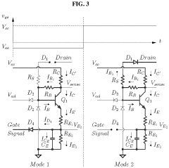
The optimization of gate resistance represents a critical balancing act in SiC MOSFET applications. While lower gate resistance enables faster switching and reduced switching losses, it simultaneously increases voltage overshoots, ringing, and EMI emissions. Conversely, higher gate resistance reduces these issues but increases switching losses and heating. Many designs now implement asymmetric gate resistance configurations, with different values for turn-on and turn-off paths to optimize this tradeoff.
The high switching speeds inherent to SiC MOSFETs create substantial challenges in gate drive design. With switching transitions occurring in nanoseconds, parasitic inductances in the gate drive loop become critical factors. Even small inductances of 5-10 nH can generate voltage spikes exceeding 20V during high di/dt events, potentially damaging the gate oxide or causing unintended turn-on/off events. This necessitates extremely careful PCB layout and component selection to minimize loop inductances.
Gate oxide reliability represents another major concern. SiC MOSFETs typically feature thinner gate oxides with lower breakdown voltages compared to silicon counterparts. The recommended gate voltage range is narrower, typically +15V/-5V or +18V/-4V, requiring more precise voltage regulation in the gate driver. Voltage overshoots during switching transitions must be strictly controlled to prevent premature oxide degradation.
The higher threshold voltages and lower transconductance of SiC MOSFETs demand robust gate drive circuits capable of delivering sufficient current to achieve optimal switching performance. Gate drivers must provide peak currents of 4-10A to charge and discharge the gate capacitance rapidly. This requirement increases complexity in driver selection and thermal management considerations.
Common-mode noise immunity presents a significant challenge in SiC MOSFET applications. The high dv/dt rates (often exceeding 50V/ns) can couple through parasitic capacitances, potentially causing false triggering or disrupting control signals. Gate drivers must incorporate advanced common-mode transient immunity (CMTI) features, typically requiring capabilities of 100V/ns or higher.
Temperature sensitivity adds another layer of complexity. SiC MOSFET threshold voltages and switching characteristics vary significantly across operating temperature ranges. Gate drive circuits must accommodate these variations to maintain consistent switching performance from -40°C to 175°C, often necessitating temperature compensation mechanisms.
The optimization of gate resistance represents a critical balancing act in SiC MOSFET applications. While lower gate resistance enables faster switching and reduced switching losses, it simultaneously increases voltage overshoots, ringing, and EMI emissions. Conversely, higher gate resistance reduces these issues but increases switching losses and heating. Many designs now implement asymmetric gate resistance configurations, with different values for turn-on and turn-off paths to optimize this tradeoff.
Current Gate Resistance Optimization Methodologies
01 Gate resistance optimization for SiC MOSFET switching performance
The gate resistance in SiC MOSFETs significantly impacts switching performance, including turn-on and turn-off speeds, switching losses, and electromagnetic interference (EMI). Optimizing gate resistance values helps balance switching speed against voltage overshoots and ringing. Different resistance values can be used for turn-on and turn-off paths to achieve optimal performance while maintaining safe operation within voltage limits.- Gate resistance optimization for SiC MOSFET switching performance: The gate resistance in SiC MOSFETs significantly impacts switching performance, including turn-on and turn-off speeds, switching losses, and electromagnetic interference (EMI). Optimizing gate resistance involves balancing between fast switching speeds (lower resistance) and reduced oscillations/EMI (higher resistance). Advanced gate drive designs allow for separate resistances for turn-on and turn-off paths to achieve optimal performance in high-frequency power conversion applications.
- Temperature effects on SiC MOSFET gate resistance: SiC MOSFETs exhibit temperature-dependent gate resistance characteristics that affect device performance across operating conditions. Gate resistance values may need to be adjusted to compensate for temperature variations, ensuring stable operation across wide temperature ranges. Temperature compensation techniques in gate drive circuits help maintain consistent switching behavior and reliability in high-temperature environments where SiC devices are often deployed.
- Integrated gate resistance solutions for SiC power modules: Advanced SiC MOSFET power modules incorporate integrated gate resistance structures to optimize performance at the module level. These designs feature carefully positioned gate resistors within the module package to minimize parasitic inductances and improve switching characteristics. Integrated solutions may include multiple resistor networks to provide different resistance values for various operating modes, enhancing overall system efficiency and reliability.
- Adaptive gate resistance control techniques: Adaptive gate resistance control systems dynamically adjust resistance values based on operating conditions to optimize SiC MOSFET performance. These systems employ feedback mechanisms to monitor switching parameters and automatically modify gate resistance to maintain ideal switching characteristics. Implementation may include digital controllers, analog circuits, or hybrid approaches that can respond to changes in load, temperature, or voltage conditions in real-time.
- Gate resistance design for parallel SiC MOSFET configurations: When multiple SiC MOSFETs are connected in parallel for high-current applications, gate resistance design becomes critical for ensuring current sharing and balanced switching. Individual gate resistors for each parallel device help compensate for parameter variations between devices and prevent current imbalance. Specialized gate drive topologies with carefully calculated resistance values prevent oscillations and ensure synchronized switching of all parallel devices.
02 Temperature effects on SiC MOSFET gate resistance
SiC MOSFETs experience significant changes in gate resistance characteristics across operating temperature ranges. Gate resistance designs must account for temperature-dependent behavior to maintain consistent switching performance and reliability. Some implementations include temperature compensation circuits that adjust gate drive parameters based on operating conditions to ensure stable performance across wide temperature ranges.Expand Specific Solutions03 Gate resistance network configurations for parallel SiC MOSFETs
When multiple SiC MOSFETs are connected in parallel, specialized gate resistance networks are required to ensure balanced current sharing and synchronized switching. These configurations may include individual gate resistors for each device, common gate resistors, or hybrid approaches. Proper gate resistance design in parallel configurations helps prevent oscillations, reduces current imbalance, and improves overall system reliability.Expand Specific Solutions04 Active gate driving techniques with variable resistance
Advanced gate driving techniques for SiC MOSFETs implement variable gate resistance that dynamically changes during switching transitions. These systems can adjust resistance values in real-time based on operating conditions, load changes, or specific switching phases. Active gate driving with programmable resistance helps optimize efficiency, reduce EMI, and protect against voltage spikes while maintaining fast switching speeds.Expand Specific Solutions05 Integrated gate resistance solutions for SiC MOSFET modules
Modern SiC MOSFET power modules incorporate integrated gate resistance solutions directly within the package. These designs optimize layout to minimize parasitic inductance while providing appropriate resistance values. Integrated approaches may include multiple resistance paths for separate turn-on and turn-off control, temperature sensing elements, and protection circuits, all optimized for the specific characteristics of SiC technology.Expand Specific Solutions
Key Industry Players in SiC MOSFET Technology
The SiC MOSFET gate resistance optimization market is currently in a growth phase, with an estimated market size exceeding $2 billion and projected to expand at 25-30% CAGR through 2030. The competitive landscape features established power semiconductor leaders like Wolfspeed, Mitsubishi Electric, and Toshiba dominating with mature gate driver solutions, while emerging players such as Global Power Technology and Fast SiC Semiconductor are gaining traction through innovative approaches. Technical maturity varies significantly: Wolfspeed and Fuji Electric have achieved advanced optimization techniques for dynamic gate resistance control, while companies like STMicroelectronics and Hitachi Power Semiconductor are focusing on integrated gate driver solutions that balance switching speed and EMI suppression. The technology is approaching mainstream adoption in electric vehicles and renewable energy applications.
Wolfspeed, Inc.
Technical Solution: Wolfspeed has pioneered advanced gate resistance optimization techniques for their SiC MOSFETs, implementing a dual-gate resistance design that uses different resistance values for turn-on and turn-off switching transitions. Their approach incorporates an asymmetric gate drive circuit with separate resistors for charging and discharging the gate, allowing independent control of dv/dt and di/dt rates. Wolfspeed's latest generation devices feature optimized internal gate resistance values combined with recommended external gate resistances to balance switching speed and EMI performance. Their technology includes specialized gate driver ICs with integrated temperature compensation to maintain consistent switching characteristics across operating conditions. Additionally, Wolfspeed has developed proprietary gate oxide processing techniques that improve interface quality and reduce threshold voltage shifts, enhancing the effectiveness of their gate resistance optimization.
Strengths: Industry-leading SiC substrate and epitaxy technology providing high-quality starting material; extensive experience in SiC device design and manufacturing; comprehensive design tools for customers to optimize gate resistance values. Weaknesses: Higher cost compared to silicon alternatives; requires more complex gate drive circuitry; switching performance highly dependent on PCB layout and system design.
Mitsubishi Electric Corp.
Technical Solution: Mitsubishi Electric has developed a sophisticated gate resistance optimization approach for their SiC MOSFETs that focuses on balancing switching losses and electromagnetic interference. Their technology employs a multi-stage gate drive circuit with dynamically adjustable gate resistance values that change during different phases of the switching transition. This allows for fast switching during the majority of the transition while slowing down at critical points to reduce ringing and EMI. Mitsubishi's approach includes integrated temperature and current sensing to adaptively modify gate resistance values based on operating conditions. Their latest generation devices feature an optimized internal gate mesh structure that distributes gate current more evenly across the chip, improving switching uniformity and reducing the need for higher external gate resistances. Mitsubishi has also implemented specialized gate oxide treatments to improve interface quality and reliability under high dv/dt conditions.
Strengths: Excellent balance between switching speed and EMI performance; robust design for industrial applications; strong integration with their power module packaging technology. Weaknesses: More complex implementation requiring specialized gate drivers; higher system cost; optimization parameters may need adjustment for different application conditions.
Critical Patents and Research on SiC Gate Drive Circuits
High temperature gate driver for silicon carbide metal-oxide-semiconductor field-effect transistor
PatentActiveUS11218145B2
Innovation
- A low-cost high temperature gate driver utilizing commercial-off-the-shelf discrete transistors and diodes, integrated with a robust overcurrent and under voltage lock out protection circuit, capable of operating up to 180°C, featuring a reduced propagation delay and flexible short-circuit protection, designed to minimize self-heating and enhance reliability.
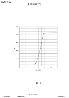
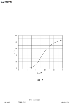
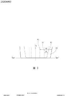
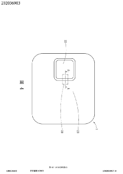
Silicon carbide semiconductor device integrating clamper circuit for clamping voltage
PatentActiveTW202036903A
Innovation
- Integration of a bidirectional voltage clamp with a silicon carbide semiconductor device, comprising a metal oxide semiconductor field effect transistor and p-type floating regions, to suppress both positive and negative overvoltages and enhance electrostatic discharge tolerance.
Thermal Management Considerations for SiC Gate Drivers
Thermal management is a critical aspect of SiC MOSFET gate driver design, particularly when optimizing gate resistance for switching performance. The higher switching frequencies and faster transition speeds of SiC MOSFETs generate significant thermal stress on gate driver components, requiring specialized thermal management strategies.
Gate resistance optimization directly impacts thermal performance in two key ways. First, lower gate resistances enable faster switching but generate higher peak currents through the gate driver, resulting in increased power dissipation and localized heating. Second, the gate driver IC itself experiences thermal stress proportional to switching frequency and gate charge, which becomes more pronounced with SiC devices operating at their performance limits.
Temperature variations significantly affect gate driver performance and reliability. Studies indicate that for every 10°C increase in operating temperature, semiconductor device lifetime may decrease by 50%. Gate drivers operating near SiC MOSFETs must withstand junction temperatures that can exceed 175°C during high-power switching events, necessitating robust thermal design considerations.
Heat dissipation techniques for gate drivers include strategic PCB layout with thermal vias, copper pour areas, and minimized trace lengths. Advanced packages like flip-chip and direct bonded copper (DBC) substrates offer superior thermal performance by reducing thermal resistance paths. Some manufacturers have introduced innovative solutions such as integrated heat spreaders within the gate driver package to manage thermal hotspots.
Thermal simulation and modeling have become essential tools in the design process. Computational fluid dynamics (CFD) and finite element analysis (FEA) enable designers to identify potential thermal issues before physical prototyping. These tools help optimize component placement and heat flow, particularly critical when balancing gate resistance values against thermal constraints.
Active cooling solutions may be necessary for high-power applications where passive cooling proves insufficient. Techniques range from forced-air cooling to liquid cooling systems for extreme power density requirements. The selection of thermally conductive materials, including specialized thermal interface materials (TIMs) with conductivities exceeding 5 W/m·K, plays a crucial role in managing heat transfer from gate driver components to cooling structures.
Monitoring and protection circuits represent another vital aspect of thermal management. Temperature sensors integrated within gate driver circuits can provide real-time feedback to control systems, enabling dynamic adjustment of switching parameters or triggering protective measures when thermal limits are approached. This adaptive approach helps maintain optimal performance while preventing thermal runaway conditions.
EMI Mitigation Strategies in SiC Switching Applications
Electromagnetic Interference (EMI) has become a critical concern in Silicon Carbide (SiC) MOSFET applications due to their inherently fast switching speeds. When optimizing gate resistance for SiC MOSFET switching, several EMI mitigation strategies must be considered to maintain system electromagnetic compatibility while preserving the performance advantages of SiC technology.
Active gate driving techniques represent one of the most promising approaches for EMI reduction. By implementing variable gate resistance during different switching phases, designers can control the switching trajectory to reduce high-frequency noise components without significantly compromising switching losses. Advanced gate drivers with programmable output impedance can dynamically adjust the gate resistance based on real-time current and voltage measurements, effectively suppressing EMI while maintaining optimal switching performance.
Physical layout optimization serves as another fundamental EMI mitigation strategy. Minimizing gate loop inductance through careful PCB design significantly reduces ringing and associated electromagnetic emissions. Implementing Kelvin source connections separates power and control current paths, reducing common-mode noise generation. Additionally, strategic placement of decoupling capacitors close to the SiC devices helps contain high-frequency switching transients within localized loops.
Passive filtering techniques complement active approaches in comprehensive EMI management. Common-mode chokes and Y-capacitors effectively attenuate common-mode noise propagation, while differential-mode filters target conducted emissions at specific frequency bands. The integration of snubber circuits—particularly RC snubbers across drain-source terminals—can dampen voltage oscillations during switching transitions, though careful design is necessary to balance EMI reduction against additional power losses.
Shielding and grounding strategies form the final layer of defense against EMI in SiC applications. Proper shielding of gate driver circuits and sensitive control components prevents radiated emissions from affecting nearby systems. Implementing a low-impedance ground plane with strategic partitioning between power and signal grounds minimizes common-mode current paths. Multi-point grounding techniques for high-frequency components combined with single-point grounding for low-frequency circuits create an effective hybrid grounding system that addresses both conducted and radiated EMI concerns.
When selecting an optimal gate resistance value, these EMI mitigation strategies must be considered holistically rather than in isolation. The ideal approach typically combines multiple techniques—balancing active gate control, layout optimization, filtering, and shielding—to achieve the required EMI performance while maintaining the switching speed advantages that make SiC MOSFETs attractive for high-efficiency power conversion applications.
Unlock deeper insights with PatSnap Eureka Quick Research — get a full tech report to explore trends and direct your research. Try now!
Generate Your Research Report Instantly with AI Agent
Supercharge your innovation with PatSnap Eureka AI Agent Platform!