

Optimizing PCB Layout For SiC MOSFET Switching Circuits
SEP 5, 202510 MIN READ
Generate Your Research Report Instantly with AI Agent
PatSnap Eureka helps you evaluate technical feasibility & market potential.
SiC MOSFET Technology Background and Objectives
Silicon Carbide (SiC) MOSFET technology represents a significant advancement in power electronics, emerging as a revolutionary alternative to traditional silicon-based semiconductors. The evolution of this technology began in the early 1990s with experimental devices, but has gained substantial momentum over the past decade due to manufacturing improvements and cost reductions. SiC MOSFETs offer superior performance characteristics including higher breakdown voltage, faster switching speeds, and better thermal conductivity compared to their silicon counterparts.
The fundamental advantage of SiC lies in its wide bandgap properties (3.26 eV compared to silicon's 1.12 eV), enabling operation at higher temperatures, voltages, and frequencies. This translates to power systems with greater efficiency, reduced cooling requirements, and smaller form factors. The technology has progressed through several generations, with each iteration addressing previous limitations in gate oxide reliability, channel mobility, and manufacturing yield.
Current market trends indicate accelerating adoption across multiple sectors including electric vehicles, renewable energy systems, industrial drives, and data center power supplies. The compound annual growth rate for SiC power devices is projected to exceed 30% through 2026, highlighting the technology's increasing importance in the power electronics landscape.
Despite these advantages, optimizing PCB layouts for SiC MOSFET switching circuits presents unique challenges due to the extremely fast switching speeds (dv/dt rates exceeding 50V/ns) and high operating frequencies. These characteristics can lead to electromagnetic interference (EMI), parasitic oscillations, and voltage overshoots that compromise system reliability and performance if not properly addressed through careful PCB design.
The primary technical objectives for optimizing PCB layouts for SiC MOSFET circuits include: minimizing parasitic inductance in the power loop to reduce switching losses and voltage overshoots; implementing effective thermal management strategies to handle the concentrated heat generation; developing gate drive circuits capable of providing clean, high-speed switching signals; and ensuring electromagnetic compatibility through appropriate shielding and layout techniques.
Additionally, there is a growing need to establish standardized design methodologies specifically tailored for SiC technology, as many existing PCB design rules developed for silicon devices prove inadequate for the switching speeds and power densities achievable with SiC. This includes reconsidering trace widths, layer stackups, component placement strategies, and isolation techniques.
The ultimate goal of this technical research is to develop comprehensive PCB layout guidelines that enable engineers to fully leverage the performance benefits of SiC MOSFETs while mitigating their inherent challenges, thereby accelerating the broader adoption of this transformative technology across various power electronics applications.
Market Demand Analysis for SiC Power Electronics
The Silicon Carbide (SiC) power electronics market is experiencing unprecedented growth, driven by the increasing demand for high-efficiency power conversion systems across multiple industries. Current market analysis indicates that the global SiC power device market is projected to reach $2.5 billion by 2025, growing at a CAGR of approximately 30% from 2020. This remarkable growth trajectory is primarily fueled by the superior properties of SiC MOSFETs compared to traditional silicon-based devices, including higher switching speeds, lower switching losses, and better thermal conductivity.
The automotive sector represents the largest market segment for SiC power electronics, particularly in electric vehicle (EV) applications. The transition toward electrification has created substantial demand for more efficient power conversion systems that can extend vehicle range, reduce charging times, and minimize thermal management requirements. Major automotive manufacturers have already begun incorporating SiC technology in their inverter designs, with some reporting efficiency improvements of 5-10% compared to silicon-based alternatives.
Renewable energy systems constitute another significant market driver for SiC power electronics. Solar inverters and wind power converters benefit tremendously from SiC MOSFETs' ability to operate at higher frequencies and temperatures, resulting in smaller passive components and reduced cooling requirements. Industry reports suggest that SiC-based solar inverters can achieve efficiency ratings exceeding 99%, representing a critical advantage in large-scale installations where even fractional efficiency improvements translate to substantial energy and cost savings.
Industrial motor drives represent the third major application area, with the market increasingly adopting SiC technology to improve energy efficiency and reduce system size. Variable frequency drives utilizing SiC MOSFETs can operate with switching frequencies 5-10 times higher than traditional IGBT-based systems, enabling more precise motor control while reducing losses by up to 30%.
Regional analysis reveals that Asia-Pacific currently dominates the SiC power electronics market, accounting for approximately 45% of global demand. This is primarily due to the region's strong manufacturing base for automotive and consumer electronics. North America and Europe follow closely, with particularly strong growth in EV and renewable energy applications.
Market challenges include the relatively higher cost of SiC devices compared to silicon alternatives and the specialized PCB layout expertise required to fully leverage SiC's high-speed switching capabilities. Current SiC MOSFETs typically command a 2-3x price premium over silicon counterparts, though this gap is narrowing as production volumes increase. Additionally, the market faces supply chain constraints, with limited SiC wafer production capacity struggling to meet rapidly growing demand.
Looking forward, industry analysts predict continued market expansion as manufacturing economies of scale reduce costs and as design expertise in optimizing PCB layouts for SiC applications becomes more widespread. The market is expected to reach maturity by 2030, by which time SiC technology will likely have displaced silicon in most high-power, high-frequency applications.
Current PCB Layout Challenges for SiC MOSFETs
Silicon Carbide (SiC) MOSFETs represent a significant advancement in power semiconductor technology, offering superior performance compared to traditional silicon-based devices. However, their implementation in switching circuits presents unique PCB layout challenges that must be addressed to fully leverage their capabilities.
The primary challenge stems from SiC MOSFETs' extremely fast switching speeds, with rise and fall times often below 10ns. This rapid switching generates high dv/dt and di/dt rates that can exceed 50V/ns and 1A/ns respectively, creating significant electromagnetic interference (EMI) and potentially disrupting nearby sensitive components if not properly managed through layout techniques.
Parasitic inductances in PCB traces become particularly problematic with SiC devices. Even small trace inductances of 10-20nH can create voltage spikes exceeding 100V during switching transitions, potentially damaging components and increasing switching losses. The traditional layout approaches developed for silicon devices often prove inadequate for these higher-frequency operations.
Gate drive circuit layout presents another critical challenge. SiC MOSFETs typically require higher gate voltages (+15V/-5V compared to +10V/0V for silicon) and are more sensitive to gate ringing. Improper gate drive layout can lead to false triggering, increased switching losses, or even device failure. The physical separation between gate driver ICs and MOSFETs must be minimized while maintaining proper isolation.
Thermal management considerations are heightened with SiC MOSFETs. While these devices offer better thermal performance than silicon counterparts, their compact size and high power density create concentrated heat sources that demand sophisticated thermal design. Inadequate thermal pathways in PCB layout can lead to hotspots and reliability issues despite SiC's theoretical temperature advantages.
Common-mode current paths present unique challenges in SiC-based designs. The high dv/dt rates can couple through parasitic capacitances to create common-mode currents that interfere with control circuits and nearby systems. Layout techniques must address these paths through careful component placement, strategic ground plane design, and sometimes dedicated filtering.
Signal integrity for control and sensing circuits becomes more critical with SiC implementations. The electromagnetic environment created by fast-switching SiC devices can corrupt analog sensing signals and digital control lines if proper isolation and shielding aren't incorporated into the PCB layout.
Additionally, SiC MOSFETs often operate at higher switching frequencies (100kHz-1MHz) than silicon equivalents, making layout considerations for skin effect and proximity effect more relevant. Trace geometries that work well at lower frequencies may create unexpected resistance and inductance at these higher operating frequencies.
Current PCB Layout Optimization Techniques
01 Gate Drive Circuit Design for SiC MOSFETs
Optimizing gate drive circuits is crucial for SiC MOSFET performance in PCB layouts. This includes proper gate resistor selection, minimizing gate loop inductance, and implementing appropriate gate voltage levels. The gate drive design must account for the faster switching speeds of SiC devices compared to traditional silicon MOSFETs, requiring careful consideration of driver placement, trace routing, and component selection to reduce parasitic effects and ensure clean switching transitions.- Gate driver circuit layout optimization: Optimizing the gate driver circuit layout is crucial for SiC MOSFET performance. This includes minimizing the gate loop inductance, proper placement of gate driver components, and using dedicated power planes. The layout should ensure short connections between the gate driver and MOSFET gate to reduce parasitic inductance and ringing. Proper decoupling capacitors placement near the gate driver helps maintain stable voltage levels during switching transitions, improving overall switching performance and reducing electromagnetic interference.
- Power loop design considerations: The power loop design is critical for SiC MOSFET PCB layouts as it affects switching performance and EMI. Minimizing the power loop area and path inductance helps reduce voltage overshoots and ringing. This can be achieved through component placement optimization, where the DC-link capacitors are placed as close as possible to the SiC MOSFETs. Using wide, short traces or copper planes for high-current paths and implementing multilayer PCB designs with dedicated power and ground planes further reduces parasitic inductance in the power loop.
- Thermal management strategies: Effective thermal management is essential for SiC MOSFET reliability and performance. PCB layouts should incorporate thermal vias under MOSFET packages to efficiently transfer heat to other layers or heatsinks. Copper pour areas can be increased around high-power components to improve heat dissipation. The layout should consider component spacing to prevent thermal coupling between heat-generating elements. Advanced cooling solutions such as integrated cooling channels or specialized thermal interface materials can be incorporated into the PCB design to handle the high power density of SiC MOSFET applications.
- EMI reduction techniques: Reducing electromagnetic interference is a major consideration in SiC MOSFET PCB layouts due to their fast switching speeds. Techniques include implementing proper grounding schemes with separate power and signal grounds connected at a single point, using ground planes to provide low-impedance return paths, and incorporating EMI filters strategically placed near noise sources. Shield traces and guard rings can be used to isolate sensitive signal paths. Component placement should minimize coupling between high-frequency switching nodes and sensitive control circuits, while careful routing of critical signals helps maintain signal integrity.
- Advanced layout automation and simulation: Advanced PCB layout automation tools and simulation techniques are increasingly important for optimizing SiC MOSFET designs. These include electromagnetic field simulators to analyze parasitic effects, thermal simulation tools to predict hotspots, and automated layout generators specifically designed for power electronics. Machine learning algorithms can be employed to optimize component placement and routing based on electrical and thermal constraints. Pre-layout and post-layout simulations help verify design performance before manufacturing, reducing development cycles and improving reliability of the final product.
02 Power Loop Layout Optimization
The power loop layout is critical for SiC MOSFET performance, requiring minimization of parasitic inductance in the DC bus and switching paths. This involves placing decoupling capacitors close to the MOSFETs, using wide and short traces for high-current paths, and implementing proper layer stacking in the PCB design. Optimized power loop layouts reduce voltage overshoots, switching losses, and electromagnetic interference, enabling the full performance potential of SiC devices to be realized.Expand Specific Solutions03 Thermal Management Strategies
Effective thermal management is essential for SiC MOSFET reliability in PCB designs. This includes implementing copper pours for heat spreading, strategic placement of thermal vias, and optimizing component placement to facilitate airflow. Advanced cooling solutions such as integrated heatsinks, thermal interface materials, and dedicated cooling channels may be incorporated into the PCB design to handle the high power density and heat generation of SiC devices, ensuring long-term reliability and performance.Expand Specific Solutions04 EMI Mitigation Techniques
SiC MOSFETs' fast switching speeds generate significant electromagnetic interference (EMI), requiring specialized PCB layout techniques for mitigation. These include implementing proper ground planes, minimizing current loop areas, using guard traces, and strategic component placement. Shielding structures, common-mode filters, and careful routing of sensitive signal traces help reduce both conducted and radiated emissions. Proper EMI design considerations ensure compliance with regulatory standards while maintaining the performance advantages of SiC technology.Expand Specific Solutions05 Advanced PCB Materials and Manufacturing Techniques
Specialized PCB materials and manufacturing techniques enhance SiC MOSFET performance. High-temperature substrates, low-loss dielectrics, and thick copper layers accommodate the unique characteristics of SiC devices. Advanced manufacturing processes like embedded components, direct bonded copper, and multilayer structures with optimized impedance control improve thermal performance and electrical characteristics. These materials and techniques enable higher power density, better reliability, and improved switching performance in SiC-based power electronics applications.Expand Specific Solutions
Leading Manufacturers in SiC MOSFET Industry
The SiC MOSFET switching circuit layout optimization market is in a growth phase, with increasing adoption across power electronics applications. The market is expanding rapidly, projected to reach significant scale as industries transition to more efficient power solutions. Technologically, the field is maturing with companies like ROHM, Mitsubishi Electric, and Fuji Electric leading innovation in SiC MOSFET design and implementation. These established players are competing with emerging specialists such as Wuxi NCE Power and Chengdu FuSemi Technology. Academic institutions including University of Electronic Science & Technology of China and Huazhong University are contributing significant research. The competitive landscape features both traditional power semiconductor manufacturers and new entrants focused specifically on SiC technology, with collaboration between industry and academia accelerating technological advancement and commercial applications.
ROHM Co., Ltd.
Technical Solution: ROHM has developed advanced PCB layout optimization techniques specifically for SiC MOSFET switching circuits that focus on minimizing parasitic inductance and capacitance. Their approach includes strategic gate driver placement with ultra-short connections to minimize loop inductance, which has been shown to reduce switching losses by up to 30%. ROHM implements specialized power loop designs with laminated bus structures that maintain low inductance paths between DC link capacitors and SiC MOSFETs. Their thermal management integration directly incorporates cooling solutions into the PCB design, with thermal vias and copper planes that efficiently dissipate heat from SiC devices. ROHM's designs also feature EMI mitigation through careful routing and shielding techniques, including the use of ground planes and strategic component placement to minimize electromagnetic interference. Their PCB layouts incorporate Kelvin source connections that separate power and signal grounds to prevent gate signal distortion during high-speed switching events.
Strengths: Industry-leading expertise in SiC device characteristics allowing for optimized switching performance; comprehensive approach that addresses electrical, thermal, and EMI concerns simultaneously. Weaknesses: Their solutions may require more complex manufacturing processes and potentially higher production costs compared to traditional layouts.
Mitsubishi Electric Corp.
Technical Solution: Mitsubishi Electric has pioneered multi-layer PCB designs for SiC MOSFET applications that strategically distribute power and signal layers to minimize interference. Their approach features dedicated power planes with optimized current paths that reduce loop areas by up to 40% compared to conventional designs. Mitsubishi's layout methodology incorporates advanced 3D electromagnetic simulation to identify and mitigate potential hotspots and EMI sources before physical implementation. Their designs implement specialized gate drive circuits with precise impedance matching and controlled slew rates, allowing for fine-tuning of switching characteristics based on application requirements. Mitsubishi has developed proprietary decoupling capacitor arrangements that provide stable power supply under high dv/dt conditions typical in SiC switching. Their PCB layouts also feature integrated temperature sensors and monitoring circuits strategically placed near critical components to enable real-time thermal management and protection.
Strengths: Comprehensive simulation-driven design approach that predicts and optimizes performance before manufacturing; excellent balance between switching speed and EMI control. Weaknesses: Solutions may be more oriented toward higher-power industrial applications, potentially overengineered for lower-power consumer applications.
Critical Design Considerations for SiC Switching Circuits
A layout method of sic MOSFET converter and SiC MOSFET converter
PatentActiveCN110266179B
Innovation
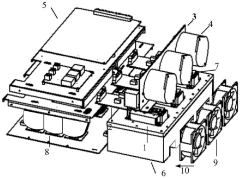
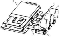
- The SiC MOSFET drive module is directly inserted into the gate-source of the SiC MOSFET module. The controller and the SiC MOSFET drive module are connected on the same side of the DC busbar, located above the three-phase inductor. The U-shaped busbar is used to connect the AC port to the three-phase inductor. Slots are opened on the radiator to facilitate the passage of busbars, and fans are installed for heat dissipation.
Designated MOSFET and driver design to achieve lowest parasitics in discrete circuits
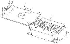
PatentInactiveUS7721232B2
Innovation
- A custom pin configuration for MOSFET transistors and drivers is implemented, with complementary package configurations to minimize circuit vias, trace segments, and interconnections, along with an integral heat sink plate for thermal conduction, optimizing the PCB layout and reducing parasitic elements.
Thermal Management Strategies for SiC Applications
Silicon Carbide (SiC) MOSFETs operate at significantly higher temperatures than traditional silicon devices, necessitating specialized thermal management strategies. Effective thermal management is critical for SiC applications as these devices can function at junction temperatures up to 200°C, compared to silicon's typical 150°C limit. This higher operating temperature creates both opportunities and challenges for PCB design engineers.
The primary thermal management approaches for SiC MOSFET circuits include active cooling systems, passive heat dissipation, and thermal interface materials optimization. Active cooling solutions typically involve forced-air or liquid cooling systems that efficiently remove heat from high-power density areas. For SiC applications, liquid cooling has shown superior performance, providing thermal resistance values as low as 0.1°C/W compared to 0.3-0.5°C/W for advanced forced-air systems.
Passive heat dissipation techniques focus on optimizing heat sink design and thermal vias placement. SiC-specific heat sinks often feature increased surface area and specialized fin structures to accommodate the higher heat flux. Thermal vias, when properly implemented in SiC applications, should be arranged in grid patterns beneath power devices with optimal diameter-to-pitch ratios of 1:2 to maximize heat transfer while maintaining structural integrity.
Material selection plays a crucial role in SiC thermal management. Advanced thermal interface materials (TIMs) with thermal conductivity exceeding 5 W/mK are recommended for SiC applications. Ceramic-filled silicone compounds and phase-change materials have demonstrated superior performance in maintaining thermal contact under the high-temperature cycling typical of SiC operations.
PCB substrate selection must also be reconsidered for SiC applications. Traditional FR-4 materials (Tg of 130-140°C) are inadequate for many SiC designs. High-temperature substrates such as polyimide (Tg >250°C) or ceramic-based materials offer better thermal stability and conductivity, though at increased cost. Metal-core PCBs provide another viable option, offering thermal conductivity up to 380 W/mK compared to FR-4's 0.3 W/mK.
Temperature monitoring and protection circuits represent another critical aspect of SiC thermal management. Implementing distributed temperature sensors with response times under 10ms helps prevent thermal runaway conditions. These systems should be coupled with intelligent gate drivers capable of adjusting switching parameters based on temperature feedback, optimizing performance while maintaining safe operating conditions.
Simulation and modeling tools specifically calibrated for SiC thermal characteristics have become essential for predicting hotspots and optimizing thermal management strategies before physical prototyping. Advanced computational fluid dynamics (CFD) models that account for SiC's unique thermal properties enable more accurate temperature distribution forecasting across complex PCB layouts.
EMI/EMC Compliance in High-Switching Frequency Designs
The increasing adoption of Silicon Carbide (SiC) MOSFETs in high-frequency switching applications has intensified the challenges related to electromagnetic interference (EMI) and electromagnetic compatibility (EMC). These wide bandgap devices, while offering superior switching performance, generate significant electromagnetic noise that must be properly managed to meet regulatory standards and ensure reliable system operation.
High-frequency switching circuits utilizing SiC MOSFETs typically operate at frequencies ranging from 100 kHz to several MHz, with extremely fast switching transitions (dv/dt rates exceeding 50V/ns). These rapid transitions create broadband electromagnetic emissions that can propagate through conducted and radiated paths, potentially interfering with nearby electronic systems and violating EMI/EMC regulations such as FCC Part 15, CISPR 22, or IEC 61000.
PCB layout optimization plays a critical role in achieving EMI/EMC compliance. The implementation of proper grounding techniques represents one of the most fundamental aspects of EMC-compliant designs. A multi-layer PCB with dedicated ground planes provides low-impedance return paths for high-frequency currents, significantly reducing common-mode emissions. The strategic placement of ground vias around high-speed signal traces further contains electromagnetic fields within defined boundaries.
Component placement strategies also significantly impact EMI performance. Placing gate drivers as close as possible to SiC MOSFETs minimizes gate loop inductance, reducing ringing and associated emissions. Similarly, input and output filtering components should be positioned to minimize the physical area of high dv/dt loops, thereby reducing their antenna effect.
Advanced PCB layout techniques such as guard traces and shield traces can provide additional EMI suppression. These structures, when properly connected to ground planes, create Faraday cage-like effects that contain electromagnetic fields. For particularly sensitive circuits, compartmentalization using shield walls or dedicated ground structures may be necessary to achieve compliance with stringent EMC standards.
Testing methodologies for EMI/EMC compliance include near-field scanning, conducted emissions measurements, and radiated emissions testing in anechoic chambers. Pre-compliance testing during the development phase can identify potential issues before formal certification, saving considerable time and resources. Software simulation tools that model electromagnetic field propagation can further assist in predicting EMI hotspots before physical prototyping.
Regulatory compliance frameworks vary by region and application, with standards such as EN 55022/CISPR 22 for information technology equipment and ISO 7637 for automotive applications. Understanding these requirements early in the design process ensures that PCB layout decisions align with compliance objectives, preventing costly redesigns and certification delays.
Unlock deeper insights with PatSnap Eureka Quick Research — get a full tech report to explore trends and direct your research. Try now!
Generate Your Research Report Instantly with AI Agent
Supercharge your innovation with PatSnap Eureka AI Agent Platform!