Impact Of SiC MOSFETs On Electric Vehicle Inverter Design
SEP 5, 20259 MIN READ
Generate Your Research Report Instantly with AI Agent
Patsnap Eureka helps you evaluate technical feasibility & market potential.
SiC MOSFET Evolution and EV Inverter Goals
Silicon Carbide (SiC) MOSFET technology has undergone significant evolution since its commercial introduction in the early 2010s. Initially, SiC devices were primarily limited to niche applications due to high production costs and reliability concerns. The first generation of commercial SiC MOSFETs offered switching frequencies around 20-50 kHz with on-resistance values significantly higher than today's standards. These early devices demonstrated the potential of wide bandgap semiconductors but had limited market penetration in automotive applications.
The technology evolution accelerated between 2015-2018, when second-generation SiC MOSFETs emerged with improved gate oxide reliability, reduced on-resistance, and enhanced thermal performance. This period marked the beginning of serious consideration for SiC implementation in electric vehicle powertrains, as the theoretical advantages of higher efficiency and power density began to materialize in practical applications.
By 2020, third-generation SiC MOSFETs achieved switching speeds exceeding 100 kHz while maintaining excellent thermal characteristics, enabling a fundamental rethinking of EV inverter designs. The progression from silicon-based IGBTs to SiC MOSFETs represents one of the most significant technological shifts in power electronics for electric vehicles in recent years.
Current technology trends indicate continued improvement in SiC wafer quality, reduction in defect density, and increasing wafer diameters (from 4-inch to 6-inch and now 8-inch), all contributing to steady cost reductions and performance enhancements. The roadmap suggests that by 2025-2026, SiC MOSFETs will achieve on-resistance values approaching theoretical limits while offering even higher temperature operation capabilities.
The primary goals for SiC MOSFET implementation in EV inverters center around several key performance metrics. First, efficiency improvements of 3-5% compared to silicon-based solutions are targeted, which directly translates to extended vehicle range. Second, power density increases of 40-50% aim to reduce inverter size and weight, creating valuable space and weight savings in vehicle design.
Temperature performance represents another critical goal, with SiC-based inverters targeting reliable operation at junction temperatures of 175-200°C, compared to the 150°C limitation of silicon devices. This higher temperature capability enables simplified cooling systems and further contributes to overall system miniaturization.
Additionally, SiC technology aims to enable higher switching frequencies (>100 kHz) in EV applications, allowing for smaller passive components and further size reductions. The ultimate technical objective is to develop inverter systems that deliver more than 100 kW/L power density while maintaining 98%+ efficiency across the operating range, supporting the next generation of electric vehicles with extended range, faster charging capabilities, and reduced system costs.
EV Market Demand for SiC-Based Inverters
The electric vehicle (EV) market is experiencing unprecedented growth, with global sales surpassing 10 million units in 2022, representing a 55% increase year-over-year. This rapid expansion has intensified the demand for more efficient power electronics, particularly inverters that can maximize vehicle range, reduce charging times, and lower overall system costs.
Silicon Carbide (SiC) MOSFET-based inverters are emerging as a critical technology to meet these market demands. Traditional silicon-based inverters are increasingly unable to satisfy the performance requirements of modern EVs, creating a significant market pull for SiC alternatives. Market research indicates that the automotive SiC power semiconductor market is projected to grow at a CAGR of 30% through 2028, reaching a market value of $7.5 billion.
Major automotive manufacturers are driving this demand through strategic commitments to electrification. Companies like Tesla, Volkswagen Group, and BYD have announced plans to incorporate SiC technology in their next-generation EV platforms. Tesla's Model 3 was among the first mass-market vehicles to utilize SiC MOSFETs in its inverter design, setting a precedent that competitors are now following.
The demand for SiC-based inverters is particularly strong in the premium and performance EV segments, where efficiency gains directly translate to marketable improvements in vehicle range and performance. However, as production scales and costs decrease, mid-market vehicles are increasingly adopting this technology as well, expanding the total addressable market.
Regional analysis shows that China, Europe, and North America represent the largest markets for SiC-based EV inverters. China leads in terms of volume, driven by government incentives and the rapid growth of domestic EV manufacturers. Europe follows with stringent emissions regulations accelerating EV adoption and consequently the demand for advanced power electronics.
Consumer preferences are also shaping market demand, with EV buyers increasingly prioritizing longer range and faster charging capabilities—both areas where SiC technology offers significant advantages. Market surveys indicate that 78% of potential EV buyers consider range anxiety a primary concern, while 65% cite charging time as a critical factor in their purchasing decision.
The commercial vehicle sector represents another growing market segment for SiC inverters. Fleet operators are particularly sensitive to total cost of ownership calculations, where the efficiency gains and reliability improvements of SiC technology can deliver compelling economic benefits despite higher initial costs.
As battery technology continues to evolve toward higher voltages (800V and beyond), the demand for SiC-based inverters is expected to accelerate further, as the performance advantages of SiC MOSFETs become even more pronounced at these elevated voltage levels.
SiC MOSFET Technology Status and Challenges
Silicon Carbide (SiC) MOSFET technology has emerged as a revolutionary advancement in power electronics, particularly for electric vehicle (EV) applications. Currently, the global SiC power device market is experiencing rapid growth, with a compound annual growth rate exceeding 30% and projected to reach $4.5 billion by 2026. This growth is primarily driven by the automotive sector, where SiC MOSFETs offer significant advantages over traditional silicon-based devices.
The current state of SiC MOSFET technology demonstrates remarkable performance characteristics, including higher breakdown voltage capabilities (typically 650V to 1700V), faster switching speeds (up to 10 times faster than silicon IGBTs), and superior thermal conductivity (approximately 3 times that of silicon). These properties enable power conversion efficiencies exceeding 98% in EV inverter applications, substantially reducing energy losses during operation.
Despite these advancements, several technical challenges persist in SiC MOSFET development. Gate oxide reliability remains a critical concern, as the interface between SiC and SiO2 contains higher defect densities compared to silicon devices. These defects can lead to threshold voltage instability and reduced device lifetime under high-temperature operation conditions typical in EV environments.
Channel mobility in SiC MOSFETs continues to be significantly lower than theoretical predictions, resulting in higher on-state resistance than ideal. This limitation stems from interface traps and surface roughness issues that have not been fully resolved in current manufacturing processes. Industry data indicates that commercial SiC MOSFETs achieve only 15-20% of the theoretical channel mobility possible with the material.
Manufacturing yield and cost factors present substantial barriers to widespread adoption. Current SiC wafer production costs remain 5-8 times higher than silicon wafers of equivalent size, with defect densities approximately an order of magnitude greater. The complex epitaxial growth processes and specialized equipment required for SiC device fabrication contribute significantly to these elevated costs.
Geographically, SiC MOSFET technology development is concentrated primarily in North America, Europe, and East Asia. The United States and Japan lead in fundamental research and intellectual property, while China has rapidly expanded manufacturing capacity. European companies have focused on automotive-specific applications, with significant investments in specialized packaging solutions designed to maximize the thermal and electrical benefits of SiC technology.
Packaging and integration challenges represent another critical area requiring innovation. Traditional packaging technologies are often inadequate for handling the high-temperature operation and rapid switching capabilities of SiC devices, leading to limitations in extracting their full performance potential in EV inverter designs.
Current SiC Inverter Design Approaches
01 SiC MOSFET Gate Drive Design
Silicon Carbide (SiC) MOSFETs require specialized gate drive designs to optimize their performance in inverter applications. These designs typically include considerations for gate voltage levels, switching speeds, and protection circuits. Proper gate drive design helps to minimize switching losses, reduce electromagnetic interference, and ensure reliable operation of SiC MOSFETs in high-frequency inverter applications. Advanced gate drive techniques may incorporate active gate control to optimize the switching trajectory and reduce stress on the device.- SiC MOSFET Gate Drive Design: Silicon Carbide (SiC) MOSFETs require specialized gate drive circuits to optimize their performance in inverter applications. These gate drivers must handle the unique switching characteristics of SiC devices, including higher switching speeds and different threshold voltages compared to traditional silicon MOSFETs. Proper gate drive design includes considerations for gate voltage levels, turn-on and turn-off speeds, and protection against voltage spikes. Advanced gate drive techniques can significantly improve the efficiency and reliability of SiC MOSFET-based inverters.
- Thermal Management for SiC Inverters: Effective thermal management is crucial for SiC MOSFET inverter designs due to the high power density and switching frequencies these devices can achieve. Cooling solutions must address the concentrated heat generation in compact inverter designs. Advanced thermal management techniques include optimized heatsink designs, phase-change materials, liquid cooling systems, and improved thermal interface materials. Proper thermal design ensures the SiC MOSFETs operate within safe temperature limits, maximizing reliability and lifetime while allowing the inverters to take full advantage of SiC's high-temperature capabilities.
- SiC MOSFET-Based Multilevel Inverter Topologies: Multilevel inverter topologies utilizing SiC MOSFETs offer advantages in high-power applications by reducing harmonic distortion, lowering switching losses, and improving output waveform quality. These designs include neutral-point-clamped (NPC), flying capacitor, and cascaded H-bridge configurations adapted specifically for SiC devices. The superior switching characteristics of SiC MOSFETs enable these multilevel inverters to operate at higher frequencies with improved efficiency compared to traditional silicon-based designs, making them particularly suitable for renewable energy systems, electric vehicle drives, and industrial motor control applications.
- EMI Mitigation in SiC Inverter Design: The fast switching speeds of SiC MOSFETs, while beneficial for efficiency, create challenges with electromagnetic interference (EMI) in inverter designs. Effective EMI mitigation strategies include optimized PCB layout techniques with minimized loop areas, strategic component placement, proper shielding, and specialized filtering components. Common mode chokes, Y-capacitors, and careful consideration of parasitic elements are essential in SiC inverter designs. Advanced gate drive techniques such as active gate driving and variable switching speeds can also help balance switching losses against EMI generation.
- Control Algorithms for SiC MOSFET Inverters: Specialized control algorithms are developed to maximize the benefits of SiC MOSFETs in inverter applications. These algorithms account for the faster switching capabilities and wider operating temperature range of SiC devices. Advanced control techniques include space vector pulse width modulation (SVPWM), model predictive control, and adaptive control strategies that optimize efficiency across varying load conditions. Dead-time compensation methods specific to SiC MOSFETs help minimize distortion and improve output waveform quality. These control strategies enable SiC inverters to achieve higher efficiency, better dynamic response, and improved reliability compared to traditional silicon-based systems.
02 Thermal Management for SiC MOSFET Inverters
Effective thermal management is crucial for SiC MOSFET inverter designs due to the high power density and switching frequencies involved. Thermal solutions may include advanced heat sink designs, liquid cooling systems, and optimized layout techniques to efficiently dissipate heat. Proper thermal management ensures the reliability and longevity of SiC MOSFET inverters by maintaining junction temperatures within safe operating limits, even under high-load conditions and in challenging environments.Expand Specific Solutions03 SiC MOSFET-Based Inverter Topologies
Various inverter topologies can be implemented using SiC MOSFETs, including half-bridge, full-bridge, and multilevel configurations. Each topology offers different advantages in terms of efficiency, power density, and control complexity. The selection of an appropriate topology depends on the specific application requirements, such as power level, voltage rating, and efficiency targets. Advanced topologies may incorporate soft-switching techniques to further reduce switching losses and improve overall system efficiency.Expand Specific Solutions04 Control Strategies for SiC MOSFET Inverters
Advanced control strategies are essential for maximizing the performance of SiC MOSFET inverters. These strategies may include space vector modulation, deadtime compensation, and model predictive control techniques. Implementing appropriate control algorithms helps to optimize switching patterns, reduce harmonic distortion, and improve dynamic response. Digital control platforms with high processing capabilities are typically used to implement these sophisticated control strategies and take full advantage of the high-speed switching capabilities of SiC MOSFETs.Expand Specific Solutions05 Protection and Reliability Enhancement for SiC MOSFET Inverters
Protection circuits and reliability enhancement techniques are critical components of SiC MOSFET inverter designs. These include overcurrent protection, overvoltage protection, and short-circuit detection mechanisms. Additionally, design considerations for improving the reliability of SiC MOSFET inverters involve addressing issues such as parasitic inductance, common-mode noise, and device degradation over time. Implementing robust protection schemes ensures safe operation under fault conditions and extends the operational lifetime of the inverter system.Expand Specific Solutions
Key SiC MOSFET Manufacturers and EV Partners
The SiC MOSFET market for electric vehicle inverters is experiencing rapid growth, transitioning from early adoption to mainstream implementation. The market is projected to expand significantly as automotive manufacturers seek higher efficiency powertrains. Technologically, industry leaders like ROHM, Mitsubishi Electric, and ON Semiconductor (Semiconductor Components Industries) have achieved commercial maturity with SiC MOSFET products, while companies such as Huawei Digital Power and Yangjie Electronic are accelerating development. Automotive manufacturers like AUDI are increasingly integrating these components into production vehicles. Academic-industry partnerships involving institutions like Beihang University and Shandong University are driving innovation in thermal management and reliability. The competitive landscape is diversifying with new entrants from China challenging established Japanese and Western suppliers.
Mitsubishi Electric Corp.
Technical Solution: Mitsubishi Electric has developed a comprehensive SiC MOSFET solution for EV inverters centered around their proprietary DMOS (Double-implanted Metal-Oxide-Semiconductor) structure with advanced trench gate design. Their latest generation SiC power modules achieve on-resistance reductions of approximately 25% compared to previous designs while maintaining high short-circuit withstand capability essential for automotive applications[1]. Mitsubishi's approach incorporates direct liquid cooling with their unique "Direct Lead Bonding" (DLB) structure that eliminates wire bonds, reducing parasitic inductance to below 8nH and enabling switching frequencies up to 80kHz in EV applications. Their SiC inverter design achieves power densities exceeding 70kW/L, representing a 40% improvement over IGBT-based systems[2]. Mitsubishi has also developed specialized gate driver ICs with active Miller clamp functionality and temperature-compensated driving parameters that optimize switching performance across the automotive temperature range (-40°C to 175°C). Their full inverter solution includes proprietary control algorithms that dynamically adjust dead time based on operating conditions, further reducing switching losses by approximately 15% compared to fixed dead-time approaches[3].
Strengths: Exceptional reliability with automotive-grade qualification; integrated solution including optimized gate drivers and control algorithms; advanced packaging technology with low thermal resistance. Weaknesses: Higher cost compared to silicon alternatives; requires more complex cooling system design; switching frequency limitations compared to some competing SiC technologies.
ROHM Co., Ltd.
Technical Solution: ROHM has developed advanced SiC MOSFET solutions specifically for electric vehicle inverters, featuring their proprietary double-trench structure that significantly reduces on-resistance while maintaining high reliability. Their fourth-generation SiC MOSFETs achieve approximately 40% reduction in switching losses compared to previous generations[1]. ROHM's technology incorporates optimized gate structures and improved cell designs that enable operation at higher switching frequencies (up to 100kHz) while maintaining thermal stability. Their SiC power modules integrate advanced packaging technology with direct liquid cooling capabilities, allowing for power densities exceeding 100kW/L in EV inverter applications[2]. ROHM has also developed specialized gate driver ICs designed specifically for SiC MOSFETs that optimize switching performance and provide robust protection features against overcurrent and short-circuit conditions, which are critical for automotive-grade reliability requirements[3].
Strengths: Industry-leading low on-resistance and switching losses; comprehensive ecosystem including gate drivers specifically optimized for SiC; established automotive qualification standards and production capacity. Weaknesses: Higher initial cost compared to silicon alternatives; requires more sophisticated thermal management systems; gate drive design is more complex requiring careful attention to prevent oscillation issues.
Critical SiC MOSFET Patents and Technical Papers
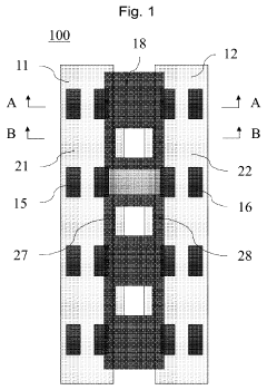
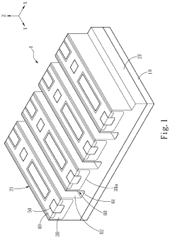
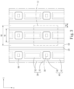
Silicon carbide metal oxide semiconductor field effect transistor and manufacturing method of silicon carbide metal oxide semiconductor field effect transistor
PatentPendingUS20230378341A1
Innovation
- The design incorporates alternating cells with specific well regions, source regions, and contact layers, including ohmic and Schottky contacts, to reduce channel density, enhance short-circuit tolerance, and minimize reverse leakage current and forward voltage drop, while maintaining the transistor's size and functionality.
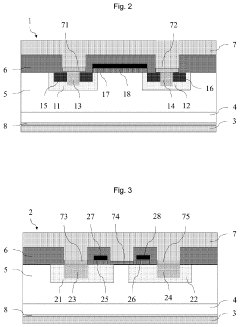
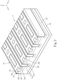
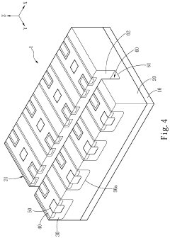
Silicon carbide semiconductor device
PatentPendingUS20240234569A9
Innovation
- A silicon carbide semiconductor device with a hybrid gate structure featuring a trench gate configuration that reduces JFET resistance and parasitic gate-to-drain capacitance, enhancing switching performance by increasing channel width density and optimizing the layout of doped regions and trenches.
Thermal Management Solutions for SiC Inverters
Thermal management represents a critical challenge in SiC-based inverter design for electric vehicles due to the unique operating characteristics of SiC MOSFETs. While these devices offer superior switching performance and efficiency compared to traditional silicon IGBTs, they generate more concentrated heat during operation, creating thermal hotspots that require innovative cooling solutions.
Liquid cooling systems have emerged as the predominant thermal management approach for SiC inverters in EVs. These systems typically employ a coolant mixture circulating through cold plates directly attached to power modules. Advanced designs feature optimized microchannel structures that maximize heat transfer surface area while minimizing pressure drop, achieving thermal resistances below 0.1 K/W in high-performance implementations.
Direct substrate cooling represents another promising approach, where the coolant directly contacts the substrate material supporting the SiC dies. This method eliminates thermal interface materials, reducing thermal resistance by up to 30% compared to conventional cold plate designs. Several EV manufacturers have begun implementing this technology in their latest models, reporting significant improvements in power density.
Two-phase cooling systems utilizing the phase change of the coolant are gaining attention for next-generation SiC inverters. These systems leverage the latent heat of vaporization to achieve heat flux capabilities exceeding 500 W/cm², substantially higher than single-phase liquid cooling. However, challenges in system complexity and control have limited widespread commercial adoption thus far.
Integration of advanced thermal interface materials (TIMs) with thermal conductivities exceeding 10 W/m·K has become essential for SiC inverter designs. Silver sintering and transient liquid phase bonding techniques are increasingly replacing traditional solder methods, reducing thermal resistance at critical interfaces by up to 50% while improving reliability under thermal cycling conditions.
Computational fluid dynamics (CFD) modeling has become indispensable in SiC inverter thermal design, enabling accurate prediction of temperature distributions and hotspots. Leading manufacturers now employ digital twin approaches that combine real-time temperature sensing with thermal models to implement dynamic thermal management strategies, optimizing performance while preventing thermal runaway conditions.
The industry trend is moving toward holistic thermal management approaches that consider the entire powertrain cooling system. Integrated cooling loops that manage inverter, motor, and battery thermal requirements simultaneously are becoming more common, with sophisticated control algorithms that balance cooling needs across components based on driving conditions and environmental factors.
Cost-Performance Analysis of SiC vs Silicon Inverters
The economic comparison between Silicon Carbide (SiC) and traditional Silicon-based inverters reveals a complex cost-performance landscape that significantly impacts electric vehicle (EV) design decisions. Initial acquisition costs for SiC MOSFETs remain approximately 2-3 times higher than their Silicon IGBT counterparts, presenting a substantial barrier to widespread adoption despite their technical advantages.
However, this cost differential must be evaluated against the considerable performance benefits SiC offers. SiC inverters demonstrate 40-50% lower switching losses and can operate at junction temperatures up to 200°C compared to Silicon's 150°C limit. These characteristics enable higher switching frequencies (20-50 kHz versus 8-15 kHz for Silicon), resulting in smaller passive components and overall inverter size reduction of 30-40%.
The total cost of ownership (TCO) analysis reveals that SiC inverters provide 3-5% improvement in vehicle range due to higher efficiency, translating to either extended driving distance or potential battery size reduction. A comprehensive financial model indicates that despite the higher initial investment, SiC inverters can achieve payback within 2-3 years of vehicle operation through energy savings and reduced cooling requirements.
Manufacturing scalability presents another critical dimension in the cost equation. As SiC wafer production volumes increase, economies of scale are gradually reducing the cost premium. Industry projections suggest SiC MOSFET costs may decrease by 10-15% annually over the next five years, potentially narrowing the cost gap with Silicon to 1.5x by 2027.
System-level redesigns enabled by SiC technology offer additional cost optimization opportunities. The higher temperature tolerance and efficiency of SiC components allow for simplified cooling systems, reducing the complexity and cost of thermal management. Furthermore, the smaller form factor enables more flexible packaging options, potentially reducing overall vehicle integration costs by 5-8%.
For mass-market EV segments, Silicon IGBTs currently maintain cost advantages that outweigh performance benefits for many manufacturers. However, in premium and performance EV segments where efficiency and power density command premium value, SiC inverters increasingly represent the preferred solution despite higher costs. This market segmentation is expected to persist until SiC manufacturing achieves greater economies of scale, with mainstream adoption accelerating as the cost differential continues to narrow.
Unlock deeper insights with Patsnap Eureka Quick Research — get a full tech report to explore trends and direct your research. Try now!
Generate Your Research Report Instantly with AI Agent
Supercharge your innovation with Patsnap Eureka AI Agent Platform!