

Comparison Between SiC MOSFETs And GaN HEMTs
SEP 5, 20259 MIN READ
Generate Your Research Report Instantly with AI Agent
PatSnap Eureka helps you evaluate technical feasibility & market potential.
SiC and GaN Power Semiconductor Evolution
The evolution of wide bandgap (WBG) power semiconductors, particularly Silicon Carbide (SiC) and Gallium Nitride (GaN), represents one of the most significant technological advancements in power electronics over the past two decades. The journey began in the early 2000s when both technologies were primarily confined to research laboratories and niche applications.
SiC technology initially gained traction in the mid-2000s, with companies like Cree (now Wolfspeed) and Infineon pioneering commercial SiC diodes. By 2010-2011, the first generation of commercial SiC MOSFETs emerged, offering switching speeds and thermal performance that significantly outperformed traditional silicon devices. The early adoption was limited by high costs and reliability concerns, particularly regarding gate oxide stability.
GaN development followed a slightly different trajectory. While research on GaN HEMTs began in the 1990s, commercial power devices only gained momentum around 2010. Early GaN devices utilized silicon substrates (GaN-on-Si) to manage costs, distinguishing them from SiC devices which used native substrates. This approach helped accelerate GaN's market entry despite initial challenges with reliability and manufacturing yield.
Between 2015-2018, both technologies experienced critical inflection points. SiC MOSFETs saw dramatic improvements in performance-to-cost ratio, with device costs decreasing by approximately 40% while performance metrics continued to improve. Concurrently, GaN HEMTs achieved significant breakthroughs in reliability and current handling capability, enabling their expansion into medium-power applications.
The automotive sector has been instrumental in driving SiC adoption, with Tesla's incorporation of SiC MOSFETs in the Model 3 inverter in 2018 marking a watershed moment. This high-profile implementation catalyzed broader industry adoption and accelerated manufacturing scale-up, further reducing costs.
GaN technology has found its strongest foothold in consumer electronics and telecommunications, where its superior high-frequency performance and miniaturization potential offer compelling advantages. The proliferation of fast-charging technologies has particularly benefited from GaN's capabilities.
Recent developments (2020-2023) show both technologies maturing rapidly. SiC has established dominance in high-power applications (>1kW), with 1200V and 1700V devices becoming mainstream in electric vehicles and industrial drives. Meanwhile, GaN has consolidated its position in lower power ranges (<1kW), with 650V devices becoming standard in compact power supplies and chargers.
Looking forward, the technological roadmap suggests continued improvements in device performance, reliability, and cost reduction. Third-generation SiC MOSFETs are emerging with enhanced ruggedness and lower switching losses, while vertical GaN structures are being developed to challenge SiC in higher power domains.
Market Demand Analysis for Wide Bandgap Semiconductors
The wide bandgap (WBG) semiconductor market is experiencing unprecedented growth driven by increasing demand for high-efficiency power electronics across multiple industries. The global WBG semiconductor market, primarily dominated by Silicon Carbide (SiC) and Gallium Nitride (GaN) technologies, was valued at approximately $1.3 billion in 2021 and is projected to reach $6.5 billion by 2028, representing a compound annual growth rate of over 25%.
This remarkable growth trajectory is fueled by several key market demands. First, the automotive sector's rapid transition toward electric vehicles (EVs) has created substantial demand for SiC MOSFETs in particular. These components enable higher power density, faster charging capabilities, and extended range through improved efficiency in power conversion systems. Major automotive manufacturers have already begun incorporating SiC technology in their EV models, with industry forecasts suggesting that by 2025, over 60% of new EVs will utilize SiC power electronics.
In parallel, the telecommunications industry is driving significant demand for GaN HEMTs, particularly for 5G infrastructure deployment. The superior high-frequency performance and power efficiency of GaN technology make it ideal for RF power amplifiers in base stations. Market analysis indicates that GaN RF device adoption in telecom infrastructure is growing at nearly 30% annually as network operators seek to optimize energy consumption while delivering higher data throughput.
Consumer electronics represents another substantial market segment, with both technologies competing for dominance. The demand for smaller, more efficient power adapters and chargers has accelerated GaN adoption in this space, with market penetration increasing from under 5% in 2020 to projected 15% by 2023. The ability of GaN to enable significantly smaller form factors while maintaining or improving efficiency has resonated strongly with consumer electronics manufacturers.
Industrial applications constitute a growing market segment for WBG semiconductors, particularly in motor drives, uninterruptible power supplies, and renewable energy systems. The industrial sector values the reliability and efficiency gains offered by both SiC and GaN technologies, with SiC currently holding a stronger position due to its higher voltage handling capabilities and thermal performance.
Regional analysis reveals that Asia-Pacific currently leads WBG semiconductor demand, accounting for approximately 45% of the global market, followed by North America at 30% and Europe at 20%. China's aggressive investment in electric vehicle manufacturing and renewable energy infrastructure has positioned it as the fastest-growing market for WBG semiconductors, with domestic demand expected to triple by 2025.
Supply chain considerations are increasingly influencing market dynamics, with recent semiconductor shortages highlighting the strategic importance of securing WBG semiconductor manufacturing capacity. This has prompted significant investments in production facilities across multiple regions, with announced capacity expansions expected to increase global output by over 200% within the next five years.
Technical Challenges in SiC MOSFETs and GaN HEMTs
Despite significant advancements in wide bandgap semiconductor technologies, both Silicon Carbide (SiC) MOSFETs and Gallium Nitride (GaN) HEMTs face distinct technical challenges that limit their full potential in power electronics applications. These challenges stem from material properties, fabrication processes, and operational requirements.
SiC MOSFETs encounter significant interface quality issues at the SiC/SiO2 boundary. The higher density of interface traps compared to traditional silicon devices leads to reduced channel mobility and reliability concerns. These interface states cause threshold voltage instability and contribute to increased on-resistance, particularly problematic in high-temperature operations where SiC devices are expected to excel.
Channel mobility degradation remains a persistent challenge for SiC MOSFETs, with typical mobility values reaching only 10-30% of theoretical predictions. This limitation directly impacts device performance by increasing conduction losses and reducing efficiency advantages over silicon counterparts.
Oxide reliability in SiC MOSFETs presents another critical challenge. The lower conduction band offset between SiC and SiO2 results in higher leakage currents and reduced breakdown strength compared to silicon devices. This becomes particularly problematic at elevated temperatures and high electric fields, conditions where SiC devices are frequently deployed.
For GaN HEMTs, current collapse phenomenon represents a major technical hurdle. This dynamic Ron increase under switching conditions is attributed to electron trapping effects that temporarily degrade device performance. Despite various passivation techniques, complete elimination of this effect remains elusive, limiting high-frequency switching applications.
Thermal management challenges are pronounced in GaN HEMTs due to the material's lower thermal conductivity compared to SiC. Localized hotspots can form during operation, potentially leading to premature device degradation or failure. This necessitates sophisticated packaging solutions that add complexity and cost to GaN implementations.
Gate reliability issues plague GaN HEMTs, particularly in enhancement-mode configurations. The lack of a native oxide comparable to silicon's SiO2 necessitates alternative gate structures that often exhibit threshold voltage instability and increased leakage currents over time and temperature cycling.
Manufacturing scalability presents challenges for both technologies. SiC wafer quality has improved but still exhibits higher defect densities than silicon, while GaN-on-Si approaches face thermal expansion mismatch issues that can introduce wafer bow and cracking during processing. These manufacturing limitations contribute to higher costs and reduced yield compared to mature silicon technologies.
Standardization and qualification frameworks lag behind silicon counterparts, creating barriers to widespread adoption. The absence of universally accepted reliability testing protocols specific to these wide bandgap technologies complicates qualification processes for mission-critical applications in automotive, aerospace, and industrial sectors.
Current Implementation Solutions and Applications
01 Device structure and fabrication of SiC MOSFETs
Silicon Carbide (SiC) MOSFETs feature unique structural designs to maximize power handling capabilities. These devices typically incorporate trench gate structures, specialized channel regions, and optimized field plate configurations to enhance breakdown voltage and reduce on-resistance. Fabrication processes include specialized thermal oxidation techniques, ion implantation methods, and annealing procedures to address the challenges of the SiC material system and improve channel mobility and gate oxide reliability.- Device structures and fabrication methods for SiC MOSFETs: Various device structures and fabrication methods have been developed to enhance the performance of SiC MOSFETs. These include specialized gate structures, channel engineering techniques, and novel doping profiles to improve carrier mobility and reduce on-resistance. Advanced fabrication processes address interface quality issues between SiC and gate dielectrics, which is crucial for reliable device operation. These innovations help overcome the challenges associated with SiC material properties while maximizing its benefits of high breakdown field and thermal conductivity.
- GaN HEMT design and performance optimization: GaN HEMTs are designed with specific structures to maximize their high-frequency and high-power capabilities. Key design elements include optimized buffer layers, advanced channel formations, and specialized gate configurations to enhance electron mobility and reduce parasitic effects. Performance optimization techniques focus on managing thermal issues, improving reliability, and increasing power density. These designs leverage GaN's wide bandgap properties to achieve superior switching speeds and efficiency compared to conventional semiconductor devices.
- Integration and packaging technologies for wide bandgap devices: Advanced packaging and integration technologies have been developed specifically for SiC MOSFETs and GaN HEMTs to address their unique thermal and electrical characteristics. These include specialized die-attach materials, innovative interconnect designs, and thermal management solutions that can handle the high power density of these devices. Integration approaches focus on minimizing parasitic inductances and capacitances to fully utilize the high-speed switching capabilities of wide bandgap semiconductors, while ensuring long-term reliability under extreme operating conditions.
- Application-specific circuit designs for power electronics: Circuit designs tailored specifically for SiC MOSFETs and GaN HEMTs maximize their advantages in power conversion applications. These include optimized gate driver circuits that address the unique switching characteristics of wide bandgap devices, protection circuits that account for their different breakdown mechanisms, and power stage topologies that leverage their high-frequency operation. The circuit designs enable higher efficiency, increased power density, and improved thermal performance in applications ranging from electric vehicle powertrains to renewable energy systems and industrial power supplies.
- Comparative analysis and hybrid utilization of SiC and GaN technologies: Research has focused on comparative analysis between SiC MOSFETs and GaN HEMTs to determine optimal applications for each technology based on their respective strengths. SiC devices typically excel in high-voltage, high-temperature applications, while GaN offers advantages in high-frequency operation. Hybrid approaches combine both technologies in complementary ways within power systems to maximize overall performance. Selection criteria include voltage ratings, switching frequency requirements, thermal considerations, and cost factors, enabling system designers to choose the most appropriate wide bandgap technology for specific application requirements.
02 GaN HEMT architecture and manufacturing techniques
Gallium Nitride (GaN) High Electron Mobility Transistors (HEMTs) employ advanced epitaxial structures with two-dimensional electron gas (2DEG) channels formed at the heterojunction interface. Key architectural elements include specialized barrier layers, field plates, and passivation schemes to manage high electric fields. Manufacturing innovations focus on substrate selection (silicon, SiC, or native GaN), buffer layer optimization, and surface treatment techniques to minimize current collapse and dynamic on-resistance issues.Expand Specific Solutions03 Packaging and thermal management solutions
Advanced packaging technologies for wide bandgap devices address the unique thermal and electrical challenges of SiC MOSFETs and GaN HEMTs. These include specialized die-attach materials with high thermal conductivity, optimized lead frame designs, and innovative interconnect technologies to minimize parasitic inductances. Thermal management solutions incorporate direct substrate cooling, advanced heat spreaders, and integrated temperature sensing to maintain device reliability under high power density operation.Expand Specific Solutions04 Gate driver and protection circuits
Specialized gate driver circuits for wide bandgap devices accommodate the unique switching characteristics of SiC MOSFETs and GaN HEMTs. These circuits feature optimized voltage levels, slew rate control, and common-mode transient immunity. Protection mechanisms include overcurrent detection with fast response times, overvoltage protection, and short-circuit handling capabilities tailored to the faster switching speeds and reduced gate charge of these devices compared to silicon alternatives.Expand Specific Solutions05 Application-specific optimization techniques
SiC MOSFETs and GaN HEMTs are optimized for specific applications through customized design approaches. For high-frequency applications, device geometries and layouts minimize parasitic capacitances and gate resistance. For high-voltage applications, edge termination structures and field management techniques enhance breakdown voltage. Power conversion applications benefit from parallel device configurations with balanced current sharing and synchronized switching to maximize efficiency and power density.Expand Specific Solutions
Key Manufacturers and Competitive Landscape
The SiC MOSFET and GaN HEMT market is currently in a growth phase, transitioning from early adoption to mainstream implementation, with a projected market size exceeding $2 billion by 2025. While SiC technology has reached higher maturity levels with established players like Wolfspeed and United Silicon Carbide leading commercial deployment in high-power applications, GaN technology is rapidly evolving with companies such as GaN Systems, Cambridge GaN Devices, and InnoScience driving innovation in medium-power segments. The competitive landscape features traditional semiconductor manufacturers (Texas Instruments, Fujitsu, Toshiba) expanding their wide bandgap portfolios alongside specialized startups. Regional competition is intensifying with strong presence from North American, European, and Asian players, particularly Chinese companies like Huawei and Yangjie Electronic investing heavily in domestic capabilities.
Wolfspeed, Inc.
Technical Solution: Wolfspeed is a leading manufacturer of SiC MOSFETs, pioneering the development of high-performance silicon carbide power devices. Their latest generation of SiC MOSFETs features a unique trench design that significantly reduces on-resistance (RDS(on)) while maintaining high blocking voltage capabilities (650V-1700V range). Wolfspeed's SiC technology delivers switching frequencies up to 100kHz with efficiency exceeding 98% in power conversion applications. Their proprietary C3M™ and C4D™ platforms incorporate advanced packaging techniques that minimize parasitic inductances, enabling faster switching transitions with reduced ringing effects. Wolfspeed's thermal management solutions allow their SiC MOSFETs to operate reliably at junction temperatures up to 175°C, significantly higher than conventional silicon devices. Their SiC MOSFETs demonstrate robust short-circuit withstand capability (typically >5μs) and positive temperature coefficient for current sharing in parallel configurations.
Strengths: Superior thermal conductivity (3x higher than GaN), higher breakdown field strength allowing higher voltage ratings (1200V-1700V standard offerings), better avalanche ruggedness, and established manufacturing ecosystem. Weaknesses: Higher gate drive voltage requirements (typically 18-20V), slower switching speeds compared to GaN HEMTs, higher cost per amp compared to silicon devices, and more complex gate drive requirements.
GaN Systems, Inc.
Technical Solution: GaN Systems specializes in gallium nitride high-electron-mobility transistors (HEMTs) with their proprietary Island Technology® that enables current handling up to 100A while maintaining extremely low on-resistance. Their GaN HEMTs operate at switching frequencies exceeding 1MHz with minimal switching losses due to near-zero reverse recovery charge. The company's GaNPX® packaging technology eliminates wire bonds and provides superior thermal performance with junction-to-case thermal resistance as low as 0.5°C/W. GaN Systems' devices feature integrated gate protection and specialized drive circuitry that simplifies implementation while ensuring reliable operation. Their enhancement-mode (e-mode) GaN transistors operate with standard gate drive voltages (0V off, 5-6V on), making them compatible with existing driver ICs. The company's GaN HEMTs demonstrate exceptional power density, achieving up to 5x higher power density compared to silicon-based solutions in applications such as power supplies, motor drives, and automotive systems.
Strengths: Extremely fast switching speeds (5-10x faster than SiC), lower gate charge requirements, zero reverse recovery losses, and higher frequency operation enabling smaller passive components. Weaknesses: Lower voltage handling capability (typically limited to 650V), less mature reliability data compared to SiC, more sensitive to overvoltage conditions, and currently limited to lateral device structures which can impact thermal performance in some applications.
Core Patents and Technical Innovations
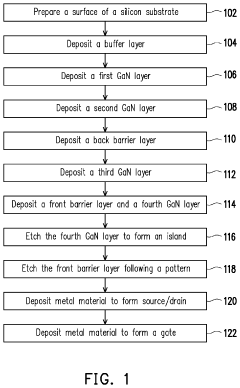
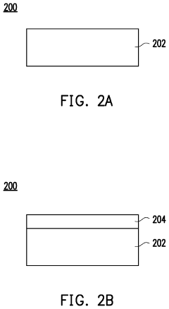
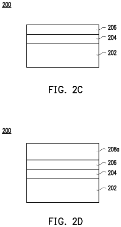
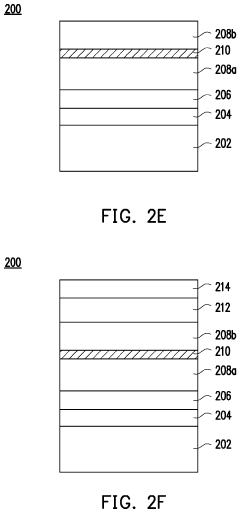
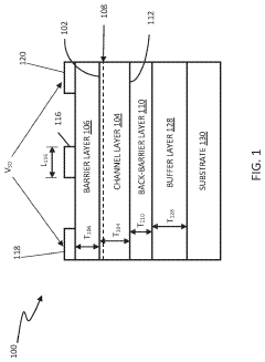
High Electron Mobility Transistor (HEMT) with a back barrier layer
PatentActiveUS11855199B2
Innovation
- The implementation of a back barrier layer in the HEMT structure, comprising group III-Nitride compounds like Aluminum (Al), Gallium (Ga), and Indium (In), is used to reduce electron leakage by effectively blocking electrons and improving electron confinement in the 2-DEG, thereby enhancing the threshold voltage and performance.
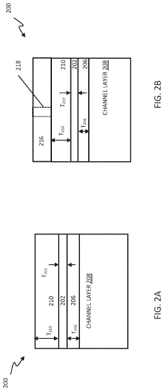
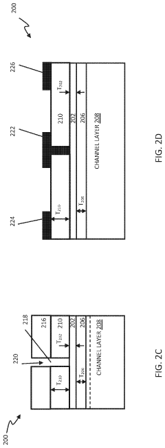
HIGH ELECTRON MOBILITY TRANSISTORS (HEMTS) INCLUDING A YTTRIUM (Y) AND ALUMINUM NITRIDE (AlN) (YAlN) ALLOY LAYER
PatentActiveUS20230223467A1
Innovation
- Incorporating a lattice-matched yttrium aluminum nitride (YAlN) alloy as a back-barrier layer in HEMTs, which has a wider bandgap than the gallium nitride channel layer, preventing secondary 2DEG formation and reducing thermal resistance, and can be used as an etch stop layer to improve electron confinement and gate control.
Thermal Management and Reliability Considerations
Thermal management represents a critical differentiator between SiC MOSFETs and GaN HEMTs, significantly impacting their reliability and performance in power electronics applications. SiC MOSFETs generally demonstrate superior thermal conductivity (approximately 3-4 W/cm·K) compared to GaN HEMTs (typically 1.3-1.5 W/cm·K), enabling more efficient heat dissipation in high-power density applications. This fundamental difference affects package design requirements and cooling system specifications across various implementation scenarios.
When examining thermal resistance pathways, SiC devices benefit from their substrate material properties, allowing for more direct thermal paths to heatsinks. Conversely, GaN HEMTs often utilize sapphire or silicon substrates with lower thermal conductivity, creating additional thermal barriers that must be addressed through advanced packaging solutions such as flip-chip configurations or integrated heat spreaders.
Temperature-dependent performance characteristics further distinguish these technologies. SiC MOSFETs maintain relatively stable performance across wider temperature ranges (-55°C to 200°C+), whereas GaN HEMTs typically show more pronounced parameter shifts at elevated temperatures, particularly regarding dynamic RDS(on) behavior. This temperature sensitivity necessitates more sophisticated thermal management strategies for GaN implementations in demanding environments.
Reliability considerations reveal distinct failure mechanisms between these technologies. SiC MOSFETs primarily contend with gate oxide integrity issues and threshold voltage instability under thermal stress, while GaN HEMTs face challenges related to current collapse phenomena and dynamic RDS(on) degradation. Long-term reliability testing indicates that SiC devices generally demonstrate more predictable aging characteristics, whereas GaN technology continues to evolve rapidly with ongoing improvements in passivation techniques and device structures to address reliability concerns.
Accelerated life testing protocols have shown that SiC MOSFETs typically achieve mean time to failure (MTTF) metrics exceeding 107 hours at rated junction temperatures, while GaN HEMTs demonstrate comparable reliability only under more constrained operating conditions. This distinction becomes particularly relevant in applications requiring extended operational lifespans such as industrial drives, renewable energy systems, and automotive powertrains.
Recent advancements in packaging technologies are progressively narrowing these thermal management gaps. Novel approaches including embedded cooling, double-sided cooling architectures, and advanced thermal interface materials are enabling both technologies to achieve higher power densities while maintaining acceptable junction temperatures. However, system designers must still carefully evaluate the thermal management requirements specific to each technology when determining optimal solutions for particular applications.
Cost-Performance Trade-offs and Economic Viability
The economic analysis of SiC MOSFETs versus GaN HEMTs reveals a complex landscape of cost-performance trade-offs that significantly impact adoption decisions across various power electronics applications. Currently, both technologies command premium pricing compared to traditional silicon devices, with SiC MOSFETs typically ranging from 3-5 times higher and GaN HEMTs 4-7 times higher than equivalent silicon MOSFETs.
Manufacturing economics play a crucial role in this cost differential. SiC benefits from more mature manufacturing processes and growing economies of scale, particularly as major suppliers like Wolfspeed, Infineon, and STMicroelectronics have expanded production capacity. GaN manufacturing remains more specialized, with fewer high-volume fabrication facilities, contributing to higher unit costs despite theoretical advantages in material utilization.
Performance benefits must be evaluated against these higher acquisition costs. SiC MOSFETs demonstrate superior economic viability in high-power applications (>1kW) where their thermal performance and reliability justify the premium. The total cost of ownership analysis frequently favors SiC when considering system-level benefits such as reduced cooling requirements, smaller passive components, and higher power density.
GaN HEMTs present compelling economics in medium-power applications (100W-1kW) where switching performance is paramount. Their superior switching characteristics enable higher frequency operation, allowing for smaller passive components and reduced overall system costs. This advantage is particularly evident in consumer electronics, data center power supplies, and automotive on-board chargers.
Market forecasts indicate a gradual cost reduction trajectory for both technologies. SiC MOSFETs are projected to decrease in price by 10-15% annually over the next five years as manufacturing capacity expands and yields improve. GaN HEMTs may experience steeper price declines of 15-20% annually as production volumes increase and manufacturing processes mature.
The economic viability inflection point varies by application. For electric vehicle traction inverters, SiC has already reached economic viability at current price points due to efficiency gains and battery size reduction benefits. For consumer electronics and lower-power applications, GaN requires further price reductions of approximately 30-40% to achieve widespread economic viability against silicon alternatives.
Regional manufacturing capabilities also influence the economic equation, with China rapidly developing domestic supply chains for both technologies to reduce dependence on imported components, potentially altering global pricing dynamics in the coming years.
Unlock deeper insights with PatSnap Eureka Quick Research — get a full tech report to explore trends and direct your research. Try now!
Generate Your Research Report Instantly with AI Agent
Supercharge your innovation with PatSnap Eureka AI Agent Platform!