Role Of SiC MOSFETs In Smart Grid And Power Distribution
SEP 5, 20259 MIN READ
Generate Your Research Report Instantly with AI Agent
Patsnap Eureka helps you evaluate technical feasibility & market potential.
SiC MOSFET Evolution and Smart Grid Integration Goals
Silicon Carbide (SiC) MOSFETs have emerged as a revolutionary technology in power electronics, marking a significant departure from traditional silicon-based devices. The evolution of SiC MOSFETs began in the early 2000s with rudimentary devices exhibiting promising characteristics but limited commercial viability. By the 2010s, manufacturing processes had matured significantly, enabling the production of more reliable and cost-effective SiC MOSFETs with superior performance metrics.
The technological trajectory of SiC MOSFETs has been characterized by continuous improvements in critical parameters such as on-resistance, switching speed, and thermal conductivity. Early generations operated at voltages around 600-1200V, while contemporary devices can handle up to 1700V with significantly reduced switching losses. This evolution has been driven by innovations in substrate quality, epitaxial growth techniques, and device fabrication processes.
In parallel with these technological advancements, the smart grid concept has evolved from traditional power distribution networks into intelligent, responsive systems capable of bidirectional power flow and real-time adaptation. The integration of renewable energy sources, energy storage systems, and electric vehicle infrastructure has created new demands for power conversion efficiency and reliability that conventional silicon devices struggle to meet.
The convergence of SiC MOSFET technology and smart grid development presents a strategic opportunity to address critical challenges in modern power distribution. The primary integration goals include enhancing energy efficiency across the grid, facilitating higher penetration of renewable energy sources, and enabling more robust and resilient power distribution networks.
Specifically, SiC MOSFETs aim to revolutionize power conversion efficiency in critical smart grid components such as solid-state transformers, grid-tied inverters, and high-voltage DC transmission systems. The target is to achieve conversion efficiencies exceeding 99% while operating at higher switching frequencies (>100 kHz) than conventional silicon devices, thereby reducing the size and weight of passive components.
Another key objective is to enhance grid resilience through improved fault tolerance and rapid response capabilities. SiC MOSFETs' superior switching characteristics enable faster fault isolation and power rerouting, potentially reducing outage durations and affected areas during grid disturbances.
The technology roadmap also emphasizes reducing the total cost of ownership for grid infrastructure by extending component lifetimes and reducing cooling requirements. While initial device costs remain higher than silicon alternatives, the trajectory suggests approaching cost parity within the next 5-7 years as manufacturing scales and yields improve.
The ultimate goal of SiC MOSFET integration into smart grid systems is to enable a more distributed, efficient, and responsive power infrastructure capable of accommodating the increasing complexity of modern energy demands while maintaining reliability and stability.
Market Demand Analysis for SiC-Based Power Distribution
The global market for Silicon Carbide (SiC) MOSFETs in smart grid and power distribution applications is experiencing unprecedented growth, driven by the increasing demand for energy-efficient power electronics solutions. The market size for SiC power devices was valued at approximately $1.1 billion in 2022 and is projected to reach $6.3 billion by 2030, representing a compound annual growth rate (CAGR) of 24.5% during the forecast period.
This remarkable growth is primarily fueled by the rapid expansion of renewable energy integration into existing power grids. As countries worldwide commit to ambitious carbon reduction targets, the installation of solar and wind power generation has accelerated, creating a substantial need for efficient power conversion and distribution technologies. SiC MOSFETs, with their superior switching characteristics and lower power losses, are increasingly becoming the preferred solution for these applications.
The electric vehicle (EV) charging infrastructure represents another significant market driver. The global EV charging station market is expected to grow at a CAGR of 30.6% from 2023 to 2030, necessitating advanced power distribution solutions. Fast-charging stations, in particular, require high-power density converters where SiC MOSFETs offer substantial advantages over traditional silicon-based alternatives.
Industrial automation and smart manufacturing sectors are also contributing to market expansion. The Industry 4.0 revolution demands more reliable and efficient power distribution systems, creating opportunities for SiC-based solutions. According to industry reports, approximately 67% of manufacturing companies are currently implementing smart factory initiatives, further driving demand for advanced power electronics.
Regional analysis reveals that Asia-Pacific currently dominates the market, accounting for approximately 45% of global demand, followed by North America and Europe. China, in particular, has emerged as both a major consumer and producer of SiC power devices, supported by government initiatives promoting semiconductor self-sufficiency and clean energy adoption.
Market segmentation by application shows that power supply and photovoltaic inverters currently represent the largest application segments for SiC MOSFETs, collectively accounting for over 50% of market share. However, the fastest growth is expected in EV charging infrastructure and industrial motor drives, with projected CAGRs exceeding 30% through 2030.
Despite the promising outlook, several factors could potentially constrain market growth. The relatively high cost of SiC devices compared to silicon alternatives remains a significant barrier to widespread adoption, particularly in price-sensitive applications. Additionally, supply chain constraints and manufacturing challenges associated with SiC wafer production have occasionally limited market expansion, though significant investments in production capacity are helping to address these issues.
Current State and Challenges of SiC MOSFETs in Power Systems
Silicon Carbide (SiC) MOSFETs have emerged as a transformative technology in power systems, with global adoption accelerating significantly over the past decade. Currently, these wide bandgap semiconductors have achieved commercial maturity in voltage ratings from 650V to 1700V, with research prototypes demonstrating capabilities up to 10kV. The market penetration of SiC MOSFETs has been particularly strong in electric vehicle inverters, solar inverters, and industrial motor drives, with compound annual growth rates exceeding 30% since 2018.
Despite this progress, SiC MOSFET technology faces several critical challenges that limit its broader implementation in smart grid and power distribution applications. The most significant technical barrier remains the gate oxide reliability issue, where the interface between SiC and SiO2 contains higher defect densities compared to traditional silicon devices. These defects lead to threshold voltage instability and reduced lifetime under high-temperature operation, particularly problematic for grid infrastructure that demands 25+ years of reliable service.
Manufacturing scalability presents another substantial challenge. Current SiC wafer production predominantly uses 6-inch wafers, while silicon technology has advanced to 12-inch wafers. This size discrepancy creates integration difficulties and cost inefficiencies when incorporating SiC devices into established semiconductor manufacturing lines. Additionally, substrate defect densities in SiC wafers remain approximately 10-100 times higher than in silicon wafers, affecting device yield and reliability.
From a geographical perspective, SiC technology development shows distinct regional characteristics. North America leads in fundamental research and intellectual property, with companies like Wolfspeed (formerly Cree) holding foundational patents. Europe has established strength in automotive and industrial applications, while Japan and China are rapidly expanding manufacturing capacity, with China particularly focused on vertically integrated supply chains from raw material to finished devices.
Cost remains a significant barrier to widespread adoption in power distribution networks. Current SiC MOSFETs typically command a 2-3x price premium over silicon IGBTs with comparable ratings. While this premium can be justified in applications where efficiency and size are paramount, it presents challenges for cost-sensitive grid infrastructure projects where initial capital expenditure often outweighs lifetime operational savings in decision-making processes.
Thermal management represents another technical hurdle. SiC devices can operate at junction temperatures up to 200°C, significantly higher than silicon's typical 150°C limit. However, existing packaging technologies, interconnection methods, and cooling systems have not fully evolved to take advantage of this capability, limiting the practical benefits in real-world power distribution applications.
Existing SiC MOSFET Implementation Solutions
01 SiC MOSFET structure and fabrication
Silicon Carbide (SiC) MOSFETs have unique structural features and fabrication methods that enhance their performance characteristics. These include specialized gate structures, channel designs, and manufacturing techniques that improve electron mobility and reduce on-resistance. The fabrication process often involves specific thermal oxidation steps, ion implantation methods, and annealing processes that are optimized for the SiC material system to achieve high-quality gate oxide interfaces and reliable device operation.- SiC MOSFET Structure and Fabrication: Silicon Carbide (SiC) MOSFETs feature unique structural designs and fabrication methods that enhance their performance characteristics. These devices typically include specialized gate structures, channel formations, and substrate configurations that contribute to their high-voltage and high-temperature capabilities. Advanced fabrication techniques are employed to create reliable SiC/oxide interfaces and to minimize defects in the crystal structure, which are critical for optimal device operation.
- Power Conversion Applications: SiC MOSFETs are extensively used in power conversion systems due to their superior switching characteristics and high efficiency. These devices enable the development of compact, high-frequency power converters with reduced energy losses. Applications include inverters, motor drives, power supplies, and renewable energy systems where their fast switching speeds and low on-resistance contribute to overall system efficiency improvements and size reduction.
- Gate Drive and Control Techniques: Specialized gate drive circuits and control techniques are essential for optimizing SiC MOSFET performance. These include advanced gate driver designs that address the unique switching characteristics of SiC devices, protection circuits to prevent overvoltage and overcurrent conditions, and control strategies that maximize efficiency while minimizing electromagnetic interference. Proper gate drive design is crucial for fully leveraging the high-speed switching capabilities of SiC MOSFETs.
- Thermal Management and Packaging: Effective thermal management and packaging solutions are critical for SiC MOSFETs operating at high power densities. Advanced packaging technologies incorporate innovative materials and designs to efficiently dissipate heat and maintain device reliability. These include specialized die-attach methods, substrate materials with high thermal conductivity, and integrated cooling solutions that enable SiC MOSFETs to operate reliably under extreme conditions while maintaining their performance advantages.
- Testing and Reliability Enhancement: Testing methodologies and reliability enhancement techniques specific to SiC MOSFETs address their unique failure modes and performance characteristics. These include accelerated stress testing, threshold voltage stability assessment, and body diode reliability evaluation. Advanced techniques for improving device robustness focus on gate oxide integrity, reducing interface traps, and enhancing surge capability. These methods are essential for ensuring the long-term reliability of SiC MOSFETs in demanding applications.
02 Power conversion applications of SiC MOSFETs
SiC MOSFETs are widely used in power conversion systems due to their superior switching characteristics and high-temperature operation capabilities. These devices enable more efficient power conversion in applications such as inverters, converters, and power supplies. The implementation of SiC MOSFETs in these systems results in reduced switching losses, higher operating frequencies, and improved thermal management, leading to smaller, more efficient power electronics systems.Expand Specific Solutions03 Gate driver designs for SiC MOSFETs
Specialized gate driver circuits are essential for optimal operation of SiC MOSFETs. These drivers are designed to handle the unique switching characteristics and gate voltage requirements of SiC devices. Advanced gate driver designs incorporate features such as adjustable slew rates, protection mechanisms against voltage spikes, and temperature compensation circuits. These optimized drivers enable faster switching speeds while maintaining safe operation, maximizing the performance benefits of SiC technology.Expand Specific Solutions04 Reliability and ruggedness improvements in SiC MOSFETs
Enhancing the reliability and ruggedness of SiC MOSFETs involves addressing specific failure mechanisms and operational stresses. Techniques include improved passivation layers, optimized field plate structures, and enhanced gate oxide quality. These improvements help mitigate issues such as threshold voltage instability, gate oxide degradation, and short-circuit capability limitations. Advanced testing methodologies and stress tests are employed to validate these reliability enhancements under extreme operating conditions.Expand Specific Solutions05 Thermal management solutions for SiC MOSFETs
Effective thermal management is crucial for SiC MOSFETs to fully utilize their high-temperature operation capability. Innovative packaging technologies, advanced cooling methods, and thermally optimized layouts are developed to dissipate heat efficiently. These solutions include direct bonded copper substrates, advanced die-attach materials, and integrated cooling structures. Proper thermal management allows SiC MOSFETs to operate at higher power densities while maintaining reliability and performance over their operational lifetime.Expand Specific Solutions
Key Industry Players in SiC MOSFET Manufacturing
The SiC MOSFET market in smart grid applications is experiencing rapid growth, currently in the early mainstream adoption phase with an estimated market size exceeding $1 billion and projected CAGR of 25-30% through 2028. Leading players include established semiconductor manufacturers like ROHM, Hitachi, and Mitsubishi Electric alongside specialized SiC innovators such as GeneSiC Semiconductor and Fast SiC Semiconductor. Major utility companies including State Grid Corp of China and China Mobile are driving implementation, while academic institutions like Xi'an Jiaotong University and Zhejiang University contribute significant research. The technology has reached commercial maturity for medium-voltage applications, though higher voltage implementations remain in development, with companies like Toshiba and Applied Materials advancing manufacturing processes to improve yield and reduce costs.
ROHM Co., Ltd.
Technical Solution: ROHM's SiC MOSFET technology for smart grid applications centers on their 4th generation trench gate structure that achieves 40% reduction in ON-resistance compared to conventional planar designs. Their SiC power modules operate at switching frequencies up to 100kHz with junction temperatures reaching 175°C, enabling more compact and efficient power conversion systems. ROHM has developed specialized gate driver ICs with built-in protection features specifically optimized for SiC MOSFET characteristics, addressing the unique switching behavior and gate drive requirements. Their integrated solutions combine SiC MOSFETs with optimized control circuitry to create complete power modules for grid-tied inverters, achieving power densities exceeding 100W/in³ and efficiency ratings above 98.5% across wide load ranges. ROHM's technology enables bidirectional power flow management essential for modern smart grid infrastructure, supporting both energy consumption and feed-in capabilities with minimal conversion losses.
Strengths: Industry-leading low ON-resistance and high-temperature operation capability provide superior efficiency in power conversion applications. Comprehensive ecosystem including optimized gate drivers ensures reliable operation. Weaknesses: Higher initial cost compared to silicon alternatives may limit adoption in cost-sensitive applications, and requires specialized design knowledge for optimal implementation.
State Grid Corp. of China
Technical Solution: State Grid's implementation of SiC MOSFET technology in smart grid applications focuses on large-scale system integration and practical deployment across their extensive distribution network. Their approach combines domestically developed SiC devices with proprietary control systems to create intelligent power electronic interfaces between transmission and distribution networks. State Grid has deployed SiC-based solid-state transformers at key substations, achieving 30% volume reduction and 15% efficiency improvement compared to conventional equipment. Their distribution automation systems leverage SiC MOSFETs' fast switching capabilities to implement advanced protection schemes with fault isolation times under 20ms, significantly improving grid reliability metrics. State Grid has pioneered the use of SiC-based power routers in their flexible distribution network architecture, enabling dynamic power flow control and optimal utilization of distributed energy resources. Their large-scale field trials have demonstrated that SiC-based power electronics can reduce distribution losses by approximately 2.5% network-wide while improving power quality metrics including THD (Total Harmonic Distortion) by up to 40%.
Strengths: Unparalleled scale of deployment provides extensive real-world operational data and validation of SiC benefits in actual grid conditions. Strong vertical integration from device specification to system implementation ensures optimized solutions. Weaknesses: Technology development sometimes prioritizes practical implementation over cutting-edge innovation, and international availability of their solutions is limited by strategic considerations.
Core Patents and Innovations in SiC Power Devices
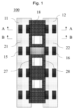
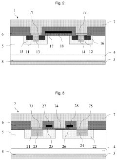
Silicon carbide metal oxide semiconductor field effect transistor and manufacturing method of silicon carbide metal oxide semiconductor field effect transistor
PatentPendingUS20230378341A1
Innovation
- The design incorporates alternating cells with specific well regions, source regions, and contact layers, including ohmic and Schottky contacts, to reduce channel density, enhance short-circuit tolerance, and minimize reverse leakage current and forward voltage drop, while maintaining the transistor's size and functionality.
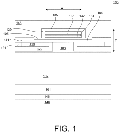
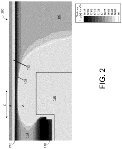
Silicon carbide field-effect transistors
PatentActiveUS20220013661A1
Innovation
- A silicon carbide (SiC) metal-oxide-semiconductor field-effect transistor (MOSFET) design incorporating a substrate, drift region, spreading layer, body region, and source region with a gate structure that includes a gate oxide layer, aluminum nitride, and p-type gallium nitride layers, achieving low on-state specific resistance and high threshold voltage.
Reliability and Lifetime Assessment of SiC MOSFETs
The reliability and lifetime assessment of SiC MOSFETs represents a critical consideration for their implementation in smart grid and power distribution systems. These devices must maintain consistent performance under various operational stresses over extended periods to justify their higher initial costs compared to traditional silicon alternatives.
Accelerated lifetime testing methodologies have been developed specifically for SiC MOSFETs, focusing on their unique failure mechanisms. These tests typically involve subjecting devices to elevated temperatures, voltage stress, and switching cycles at rates significantly higher than normal operation to predict long-term reliability. Research indicates that SiC MOSFETs can maintain operational stability for 15-20 years under proper thermal management conditions.
Threshold voltage instability remains one of the primary reliability concerns for SiC MOSFETs in grid applications. This phenomenon, characterized by shifts in threshold voltage during extended operation, can lead to unpredictable switching behavior and potential system failures. Recent studies have shown that newer generation devices exhibit improved stability through enhanced gate oxide quality and interface engineering.
Time-dependent dielectric breakdown (TDDB) of the gate oxide represents another significant reliability challenge. The higher electric fields present in SiC MOSFETs compared to silicon devices place additional stress on the gate oxide. Manufacturers have responded by implementing more robust oxide growth techniques and novel dielectric materials to enhance breakdown resistance.
Body diode degradation during reverse conduction has been identified as a reliability concern specific to SiC MOSFETs in grid applications with frequent bidirectional power flow. This degradation manifests as increased forward voltage drop and leakage current over time. Advanced device designs incorporating improved body diode structures or external anti-parallel Schottky diodes have been developed to mitigate this issue.
Environmental factors significantly impact SiC MOSFET reliability in smart grid deployments. Humidity, temperature cycling, and mechanical stress can accelerate degradation mechanisms. Hermetic packaging solutions and conformal coatings have proven effective in protecting devices from these environmental stressors, particularly in outdoor installation scenarios common in distributed energy resources.
Reliability modeling techniques have evolved to better predict SiC MOSFET lifetime in grid applications. Physics-of-failure approaches combined with statistical methods now provide more accurate lifetime estimations than traditional constant-failure-rate models. These advanced models incorporate multiple stress factors and their interactions to deliver more realistic predictions for complex operational profiles typical in modern grid systems.
Energy Efficiency and Carbon Reduction Impact
The integration of Silicon Carbide (SiC) MOSFETs in smart grid and power distribution systems represents a significant advancement in energy efficiency and carbon reduction efforts. These wide-bandgap semiconductor devices demonstrate superior performance characteristics compared to traditional silicon-based alternatives, resulting in substantial energy savings across the power distribution chain.
SiC MOSFETs enable power conversion systems to operate at higher switching frequencies with reduced switching losses, leading to efficiency improvements of 20-40% in various grid applications. This enhanced efficiency directly translates to reduced energy consumption and lower carbon emissions. For instance, in solar inverters, the implementation of SiC technology has demonstrated efficiency gains of up to 3%, which, when scaled across large solar installations, represents significant energy conservation.
The reduced conduction and switching losses of SiC MOSFETs also minimize heat generation, decreasing the cooling requirements for power electronics systems. This cascading effect further reduces energy consumption associated with thermal management, contributing to the overall carbon footprint reduction of grid infrastructure. Studies indicate that cooling system energy requirements can be reduced by up to 30% when transitioning from silicon to SiC-based power electronics.
In electric vehicle charging infrastructure, which increasingly interfaces with smart grids, SiC MOSFETs enable faster charging capabilities while maintaining high efficiency. This improvement accelerates the adoption of electric mobility solutions, further supporting decarbonization efforts in the transportation sector. The higher power density achieved with SiC technology also results in more compact charging stations, reducing material usage and associated embodied carbon.
Quantitative assessments suggest that widespread adoption of SiC technology in smart grid applications could contribute to carbon emission reductions of 5-10% in the electricity sector by 2030. This impact becomes particularly significant when considering the global scale of power distribution networks and their continuous operation.
The lifecycle carbon benefits of SiC MOSFETs extend beyond operational efficiency. Their longer operational lifespan compared to silicon devices reduces replacement frequency and associated manufacturing emissions. Additionally, their ability to operate reliably at higher temperatures expands the potential for waste heat recovery systems, creating opportunities for combined heat and power applications that further enhance overall energy utilization.
As grid modernization efforts accelerate globally, the cumulative carbon reduction impact of SiC MOSFET implementation represents a critical technological contribution to meeting international climate commitments and transitioning toward more sustainable energy systems.
Unlock deeper insights with Patsnap Eureka Quick Research — get a full tech report to explore trends and direct your research. Try now!
Generate Your Research Report Instantly with AI Agent
Supercharge your innovation with Patsnap Eureka AI Agent Platform!