High-Voltage Applications Of SiC MOSFET Modules
SEP 5, 20259 MIN READ
Generate Your Research Report Instantly with AI Agent
Patsnap Eureka helps you evaluate technical feasibility & market potential.
SiC MOSFET Evolution and High-Voltage Goals
Silicon Carbide (SiC) MOSFET technology has undergone remarkable evolution since its initial development in the early 1990s. The journey began with rudimentary devices exhibiting high on-resistance and limited voltage capabilities, typically below 1200V. These early iterations suffered from numerous reliability issues, particularly related to gate oxide integrity and threshold voltage instability under high-temperature operations.
By the mid-2000s, significant breakthroughs in material quality and fabrication processes enabled the commercial introduction of the first generation of SiC MOSFETs. These devices demonstrated improved performance with blocking voltages reaching 1200V-1700V range, making them suitable for medium voltage applications in power conversion systems.
The technological trajectory has been consistently upward, with each generation delivering enhanced performance metrics. Modern SiC MOSFETs now feature dramatically reduced specific on-resistance, improved switching characteristics, and enhanced thermal performance. This evolution has been driven by innovations in epitaxial growth techniques, device architecture optimization, and packaging technologies specifically designed to leverage SiC's inherent material advantages.
Current high-voltage goals for SiC MOSFET modules are ambitious and multifaceted. The primary objective is to push the voltage boundaries beyond 10kV while maintaining competitive on-resistance values. This represents a critical threshold for enabling SiC adoption in ultra-high-voltage applications such as HVDC transmission, traction systems for high-speed trains, and medium voltage grid infrastructure.
Another significant goal involves improving the switching performance at elevated voltages. As blocking voltage increases, maintaining fast switching speeds becomes increasingly challenging due to parasitic capacitances and inductances. Advanced module designs with optimized internal layouts and novel interconnection technologies are being developed to address these limitations.
Reliability under high-voltage stress conditions remains a paramount concern. Research efforts are focused on enhancing the robustness of gate oxide structures, improving short-circuit withstand capabilities, and ensuring stable long-term operation under repetitive switching conditions at elevated temperatures and voltages.
The roadmap for SiC MOSFET evolution also emphasizes cost reduction strategies to improve economic viability for high-voltage applications. This includes increasing wafer diameters, enhancing manufacturing yields, and developing more efficient packaging solutions that can handle the thermal and electrical requirements of high-voltage operation while reducing overall system complexity.
Market Demand for High-Voltage SiC Solutions
The global market for high-voltage SiC MOSFET modules has experienced significant growth in recent years, driven primarily by the increasing demand for efficient power conversion systems in renewable energy, electric vehicles (EVs), and industrial applications. The market value for SiC power devices reached approximately $1.1 billion in 2022 and is projected to grow at a compound annual growth rate (CAGR) of 34% through 2028, with high-voltage applications representing a substantial portion of this expansion.
The renewable energy sector presents one of the most compelling market opportunities for high-voltage SiC solutions. Solar inverters and wind power converters require increasingly efficient power electronics to maximize energy harvest and minimize conversion losses. SiC MOSFETs operating at voltages above 1.2kV have demonstrated efficiency improvements of 2-3 percentage points compared to traditional silicon-based solutions, translating to significant energy savings over system lifetimes.
Electric vehicle charging infrastructure represents another rapidly growing segment. The push toward faster charging capabilities necessitates higher voltage systems, with 800V and 1200V architectures becoming increasingly common. High-voltage SiC MOSFET modules enable more compact, efficient, and reliable charging stations capable of delivering power at rates exceeding 350kW, reducing charging times to under 15 minutes for modern EVs.
In the industrial sector, high-voltage SiC solutions are gaining traction in motor drives, uninterruptible power supplies (UPS), and high-voltage DC transmission systems. The industrial motor drive market alone is expected to incorporate SiC technology in 18% of new installations by 2025, up from just 4% in 2020, with high-voltage applications leading this transition.
Regional analysis reveals that Asia-Pacific currently dominates the market demand, accounting for 45% of global consumption, followed by Europe (30%) and North America (20%). China's aggressive push toward electrification across multiple sectors has positioned it as the single largest market for high-voltage SiC modules, with government initiatives supporting domestic production capabilities.
Customer requirements are evolving toward higher power density, improved reliability, and enhanced thermal performance. End users increasingly demand modules capable of operating at junction temperatures exceeding 200°C while maintaining reliability over 15+ year service lifetimes. This has created a premium segment within the market where performance characteristics outweigh initial cost considerations.
Despite strong growth projections, market penetration faces challenges related to supply chain constraints and cost premiums. High-voltage SiC modules typically command a 2.5-3x price premium over silicon alternatives, though this gap is expected to narrow to 1.5-2x by 2026 as manufacturing scales and yields improve.
SiC MOSFET Technology Status and Barriers
Silicon Carbide (SiC) MOSFET technology has emerged as a revolutionary advancement in power electronics, particularly for high-voltage applications. Currently, SiC MOSFETs are commercially available with voltage ratings ranging from 650V to 3.3kV, with research prototypes demonstrating capabilities up to 15kV. This represents significant progress compared to traditional silicon-based devices, which face fundamental physical limitations at higher voltages.
Despite these advancements, SiC MOSFET technology faces several critical barriers that impede its widespread adoption in high-voltage applications. The primary challenge remains the material quality of SiC wafers, which still exhibit higher defect densities compared to silicon. These defects, particularly basal plane dislocations and micropipes, significantly impact device reliability and yield, especially in larger die sizes required for high-voltage modules.
The interface quality between SiC and gate oxide presents another substantial hurdle. The higher interface trap density leads to reduced channel mobility and threshold voltage instability, which becomes more pronounced in high-voltage applications where reliability is paramount. Recent improvements in oxidation processes and post-oxidation annealing have mitigated some issues, but further refinement is necessary.
Manufacturing scalability poses a significant barrier to cost reduction. Current SiC wafer sizes predominantly remain at 6-inch diameter, while silicon technology has advanced to 12-inch wafers. This disparity in manufacturing scale contributes to the 3-5x cost premium of SiC devices compared to their silicon counterparts, limiting market penetration despite superior performance characteristics.
Packaging technology represents another critical challenge for high-voltage SiC modules. Traditional packaging materials and designs often cannot fully exploit SiC's high-temperature capabilities (potentially exceeding 200°C) and faster switching speeds. Parasitic inductances in conventional packages limit switching performance, while thermal management becomes increasingly complex at higher power densities.
Globally, SiC technology development shows distinct regional patterns. Japan and the United States pioneered early SiC research, with companies like Cree/Wolfspeed, Rohm, and Mitsubishi establishing strong patent portfolios. Europe has focused on automotive and industrial applications, while China has rapidly expanded its SiC manufacturing capacity in recent years, though still lagging in fundamental technology innovation.
Reliability verification methodologies specific to SiC devices remain underdeveloped compared to mature silicon technologies. The lack of standardized qualification procedures for high-voltage SiC modules creates uncertainty for system designers, particularly in mission-critical applications where operational lifetimes of 15-20 years are expected.
Current High-Voltage SiC Module Architectures
01 SiC MOSFET Module Design and Structure
Silicon Carbide (SiC) MOSFET modules feature specialized designs and structures to optimize performance. These modules incorporate advanced packaging techniques that enhance thermal management, reduce parasitic inductance, and improve overall reliability. The structural designs often include optimized layouts for power terminals, gate connections, and heat dissipation pathways to maximize the inherent benefits of SiC semiconductor material.- SiC MOSFET Module Design and Structure: Silicon Carbide (SiC) MOSFET modules feature specialized designs and structures to optimize performance. These modules incorporate advanced packaging techniques to enhance thermal management, reduce parasitic inductance, and improve overall reliability. The structural innovations include optimized layout designs, novel interconnection methods, and integration approaches that maximize the benefits of SiC semiconductor properties while addressing the unique challenges of high-frequency, high-temperature operation.
- Thermal Management Solutions for SiC MOSFET Modules: Effective thermal management is critical for SiC MOSFET modules due to their high-power density and operating temperatures. Various cooling technologies and materials are employed, including advanced heat sinks, thermal interface materials, direct liquid cooling systems, and innovative substrate materials with superior thermal conductivity. These solutions help dissipate heat efficiently, maintain optimal junction temperatures, and ensure long-term reliability of the modules under high-power switching conditions.
- Gate Drive and Control Circuits for SiC MOSFETs: Specialized gate drive and control circuits are essential for optimizing SiC MOSFET module performance. These circuits address the unique switching characteristics of SiC devices, including faster switching speeds and different threshold voltage requirements compared to silicon counterparts. Advanced gate drivers incorporate features such as adjustable driving voltages, active Miller clamping, desaturation protection, and temperature compensation to ensure reliable operation while maximizing the switching performance advantages of SiC technology.
- Parallel Operation and Multi-chip Integration: SiC MOSFET modules often employ parallel device operation and multi-chip integration techniques to achieve higher current ratings and power handling capabilities. These approaches require careful consideration of current sharing, switching synchronization, and balanced thermal distribution. Advanced module designs incorporate specialized interconnection methods, symmetrical layouts, and matched device characteristics to ensure uniform current distribution and switching behavior across all parallel chips, maximizing overall module performance and reliability.
- Protection and Reliability Enhancement Features: SiC MOSFET modules incorporate various protection and reliability enhancement features to ensure robust operation in demanding applications. These include short-circuit protection mechanisms, overvoltage protection circuits, temperature monitoring systems, and specialized packaging materials resistant to thermal cycling and environmental stresses. Advanced modules may also feature condition monitoring capabilities, fault detection algorithms, and graceful degradation mechanisms to prevent catastrophic failures and extend operational lifetime in high-stress power conversion applications.
02 Thermal Management Solutions for SiC MOSFET Modules
Effective thermal management is critical for SiC MOSFET modules due to their high power density and operating temperatures. Various cooling technologies are implemented, including advanced heat sink designs, direct liquid cooling systems, and novel thermal interface materials. These solutions help maintain optimal junction temperatures, prevent thermal runaway, and extend the operational lifetime of the modules while allowing them to operate at higher power densities than traditional silicon-based alternatives.Expand Specific Solutions03 Gate Drive and Control Strategies for SiC MOSFETs
Specialized gate drive circuits and control strategies are essential for SiC MOSFET modules to handle their unique switching characteristics. These include optimized gate voltage levels, advanced protection mechanisms against voltage spikes, and precise timing control for switching transitions. The gate drive solutions often incorporate temperature compensation, short-circuit protection, and active Miller clamping to ensure reliable operation across various operating conditions.Expand Specific Solutions04 Parallel Operation and Multi-chip Integration
SiC MOSFET modules often employ parallel device operation and multi-chip integration techniques to achieve higher current ratings and power handling capabilities. These approaches require careful consideration of current sharing, synchronized switching, and balanced thermal distribution. Advanced module designs incorporate specialized interconnection methods, matched device characteristics, and optimized layout patterns to ensure uniform current distribution and switching behavior across all parallel chips.Expand Specific Solutions05 Application-Specific SiC MOSFET Module Solutions
SiC MOSFET modules are designed with specific application requirements in mind, such as electric vehicles, renewable energy systems, industrial drives, and grid infrastructure. These application-specific modules feature customized voltage and current ratings, optimized switching frequencies, and tailored protection features. The module designs may incorporate additional functionality like integrated sensors, specialized cooling solutions, or specific form factors to meet the demands of particular industries or use cases.Expand Specific Solutions
Key SiC MOSFET Module Manufacturers
The SiC MOSFET modules for high-voltage applications market is in a growth phase, with increasing adoption across power electronics sectors. The market is projected to expand significantly due to rising demand in electric vehicles, renewable energy, and industrial applications. Technologically, SiC MOSFETs are maturing rapidly with companies at different development stages. Wolfspeed leads as a pioneer with comprehensive product portfolios, while Toshiba, ON Semiconductor, and Sumitomo Electric have established strong positions. Chinese players like Global Power Technology and Yangjie Electronic are rapidly advancing their capabilities. Academic institutions including Xi'an Jiaotong University and North Carolina State University are contributing significant research. The ecosystem shows a collaborative dynamic between established semiconductor manufacturers, emerging specialists, power utilities, and research institutions driving innovation in this critical power electronics technology.
Wolfspeed, Inc.
Technical Solution: Wolfspeed has pioneered SiC MOSFET technology for high-voltage applications with their advanced XM3 power modules designed specifically for 1.2kV to 3.3kV applications. Their modules feature optimized layout with low parasitic inductance and integrated temperature sensors for enhanced thermal management. Wolfspeed's latest generation modules utilize trench MOSFET technology that achieves significantly lower on-resistance compared to planar designs, resulting in power density improvements of up to 50%[1]. Their modules incorporate advanced packaging technology with direct bonded copper (DBC) substrates and silver sintering die-attach for superior thermal cycling reliability. For grid-tied applications, Wolfspeed has developed specialized gate driver solutions that provide robust short-circuit protection with response times under 2μs and active Miller clamping to prevent parasitic turn-on in high dv/dt environments[3].
Strengths: Industry-leading SiC substrate quality with lowest defect density, enabling higher yield and reliability; comprehensive vertical integration from wafer to module; extensive application expertise in high-voltage systems. Weaknesses: Higher cost compared to silicon alternatives; requires specialized gate drive design; limited high-temperature packaging options for extreme environments.
Toshiba Corp.
Technical Solution: Toshiba has developed high-voltage SiC MOSFET modules specifically designed for power transmission and industrial motor drive applications. Their modules feature a unique hybrid structure combining silicon IGBTs with SiC Schottky barrier diodes to optimize switching performance while managing costs. Toshiba's latest generation modules employ their proprietary "Super Junction" structure that significantly reduces on-resistance while maintaining high breakdown voltage capabilities up to 3.3kV[2]. The company has implemented advanced thermal management solutions including direct liquid cooling options that enable power densities exceeding 100W/cm³. Their modules incorporate specialized gate driver circuits with active Miller clamp functionality and short-circuit protection designed specifically for the switching characteristics of SiC devices. Toshiba has also developed unique packaging technology with high-reliability die bonding and reduced thermal resistance, allowing junction temperatures up to 175°C for sustained operation[4].
Strengths: Extensive experience in high-voltage power electronics; strong manufacturing capabilities ensuring consistent quality; innovative hybrid solutions balancing performance and cost. Weaknesses: Relatively late entry to full SiC module market compared to some competitors; more limited product range in ultra-high voltage (>3.3kV) applications.
Critical Patents in SiC MOSFET Technology
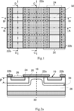
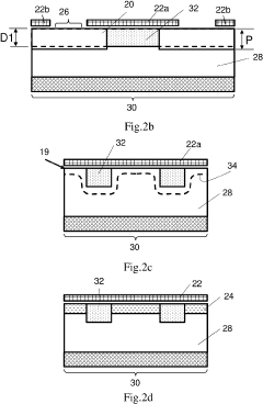
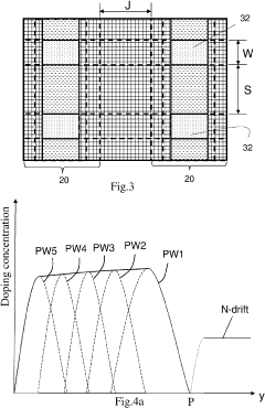
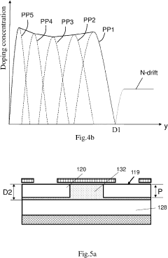
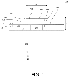
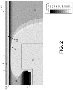
Sic mosfet with transverse p+ region
PatentActiveUS20230053874A1
Innovation
- The design incorporates a silicon carbide MOSFET structure with specific doping layers and geometries, including a polysilicon gate layer, to enhance the protection of the gate oxide without increasing the MOSFET cell area, utilizing epitaxy and ion implantation processes to create N+ and P+ regions that act as shields, ensuring adequate body diode performance and channel mobility.
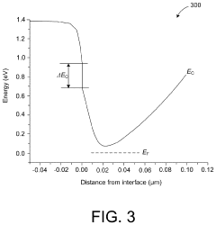
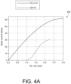
Silicon carbide field-effect transistors
PatentActiveUS20220013661A1
Innovation
- A silicon carbide (SiC) metal-oxide-semiconductor field-effect transistor (MOSFET) design incorporating a substrate, drift region, spreading layer, body region, and source region with a gate structure that includes a gate oxide layer, aluminum nitride, and p-type gallium nitride layers, achieving low on-state specific resistance and high threshold voltage.
Thermal Management Challenges
Thermal management represents one of the most critical challenges in high-voltage SiC MOSFET module applications. Despite SiC MOSFETs' superior thermal conductivity compared to silicon counterparts (approximately 3-4 times higher), the extreme power densities achieved in modern high-voltage applications create unprecedented thermal stress. Operating temperatures in these modules frequently approach 175-200°C, pushing cooling systems to their limits and accelerating device degradation mechanisms.
The junction-to-case thermal resistance pathway presents a particular bottleneck in SiC MOSFET modules. Current packaging technologies struggle to efficiently extract heat from increasingly compact die arrangements, with thermal interface materials often becoming the limiting factor. Advanced thermal interface materials such as sintered silver and copper sintering show promise but introduce manufacturing complexity and reliability concerns under thermal cycling conditions.
Hot-spot formation represents another significant thermal management challenge. The uneven current distribution characteristic of high-voltage SiC MOSFET modules creates localized heating that can exceed average junction temperatures by 15-30°C. These thermal gradients not only reduce overall system reliability but complicate accurate temperature monitoring and protection strategies. Emerging technologies utilizing embedded temperature sensors and real-time thermal imaging provide more granular monitoring but add system complexity.
Cooling system design for high-voltage SiC modules requires balancing multiple competing factors. Liquid cooling systems offer superior thermal performance but introduce reliability concerns regarding coolant leakage in high-voltage environments. Two-phase cooling technologies demonstrate exceptional heat extraction capabilities but face commercialization barriers related to cost and integration complexity. Meanwhile, air-cooled solutions remain prevalent despite their limitations due to their simplicity and established reliability record.
The thermal-electrical interaction in SiC MOSFET modules creates additional challenges. As junction temperatures rise, on-state resistance increases, generating additional heat in a potentially destructive feedback loop. This phenomenon becomes particularly problematic in high-voltage applications where switching losses are already substantial. Advanced gate driver designs incorporating temperature-compensated driving strategies show promise in mitigating these effects but require sophisticated control algorithms.
Long-term reliability under thermal cycling represents perhaps the most significant unresolved challenge. The coefficient of thermal expansion mismatch between SiC dies, substrates, and packaging materials creates mechanical stress during thermal cycling. This stress manifests as solder fatigue, bond wire lift-off, and die attach degradation. While advanced packaging technologies like silver sintering and pressure-assisted sintering demonstrate improved reliability, they significantly increase manufacturing costs and complexity.
Reliability Testing Standards
Reliability testing standards for SiC MOSFET modules in high-voltage applications are critical to ensure operational safety, performance consistency, and longevity under extreme conditions. These standards have evolved significantly to address the unique characteristics of silicon carbide technology, which operates at higher temperatures, voltages, and switching frequencies than traditional silicon-based devices.
The Joint Electron Device Engineering Council (JEDEC) has established several key standards specifically applicable to SiC power devices, including JESD22-A108 for temperature cycling, JESD22-A110 for highly accelerated temperature and humidity stress testing, and JESD22-A101 for steady-state temperature humidity bias life tests. These standards provide structured methodologies to evaluate device reliability under various environmental stressors.
IEC 60747-9, developed by the International Electrotechnical Commission, outlines specific requirements for power semiconductor devices, with recent amendments incorporating SiC MOSFET testing parameters. This standard addresses critical aspects such as gate oxide integrity testing, which is particularly important for SiC MOSFETs due to their thinner oxide layers compared to silicon counterparts.
Automotive Electronics Council's AEC-Q101 qualification has been adapted for wide bandgap semiconductors, including specific provisions for SiC devices used in high-voltage automotive applications. These modifications account for the higher operating temperatures (175°C and beyond) and voltage ratings (1200V-3300V) common in SiC MOSFET modules.
Short-circuit robustness testing has emerged as a crucial reliability standard, with methodologies defined to evaluate device behavior under fault conditions. The IEC 60749 series provides guidelines for these tests, requiring SiC MOSFETs to withstand short-circuit conditions for a minimum of 2-5 microseconds, depending on the application class.
Power cycling tests, as outlined in IEC 60749-34, have been modified for SiC technology to account for the higher ΔTj (junction temperature swings) these devices experience. Standard test protocols now include accelerated testing at junction temperatures up to 200°C, with some specialized tests extending to 250°C for next-generation devices.
Humidity-based reliability tests have also evolved, with HAST (Highly Accelerated Stress Testing) and H3TRB (High Humidity, High Temperature Reverse Bias) tests now conducted at more extreme conditions to account for the higher voltage ratings of SiC modules. These tests typically run for 1000 hours at 85% relative humidity and temperatures of 85-130°C while devices are under bias.
Gate oxide reliability testing has received particular attention, with specialized standards developed to address the threshold voltage instability issues unique to SiC technology. These tests typically involve extended gate bias stress under elevated temperatures to evaluate long-term stability of the gate-source threshold voltage.
Unlock deeper insights with Patsnap Eureka Quick Research — get a full tech report to explore trends and direct your research. Try now!
Generate Your Research Report Instantly with AI Agent
Supercharge your innovation with Patsnap Eureka AI Agent Platform!