

How Does Parasitic Inductance Affect SiC MOSFET Performance?
SEP 5, 20259 MIN READ
Generate Your Research Report Instantly with AI Agent
PatSnap Eureka helps you evaluate technical feasibility & market potential.
SiC MOSFET Parasitic Inductance Background and Objectives
Silicon Carbide (SiC) MOSFET technology has emerged as a revolutionary advancement in power electronics over the past two decades. The evolution of this wide bandgap semiconductor material represents a significant departure from traditional silicon-based devices, offering superior performance characteristics including higher breakdown voltage, faster switching speeds, and improved thermal conductivity. Since the early 2000s, SiC MOSFETs have progressed from laboratory curiosities to commercially viable components, with substantial improvements in manufacturing processes and device reliability.
The technological trajectory of SiC power devices has been marked by continuous refinement in substrate quality, epitaxial growth techniques, and device fabrication processes. Early challenges related to crystal defects and gate oxide reliability have been progressively addressed, leading to today's high-performance devices. This evolution has enabled switching frequencies that are 5-10 times higher than conventional silicon devices, with significantly reduced switching losses.
Parasitic inductance has emerged as a critical factor limiting the full potential of SiC MOSFETs. As switching speeds increase, even small inductances in the power loop and gate drive circuits can generate substantial voltage overshoots and ringing, potentially leading to device failure or electromagnetic interference issues. The relationship between parasitic inductance and device performance becomes increasingly pronounced as devices continue to improve in speed and efficiency.
The primary objective of this technical investigation is to comprehensively understand how parasitic inductance affects SiC MOSFET performance across various operating conditions. This includes quantifying the impact on switching losses, voltage overshoots, electromagnetic interference, and overall system reliability. By establishing clear correlations between parasitic elements and device behavior, we aim to develop design guidelines that maximize SiC MOSFET capabilities.
Additionally, this research seeks to identify optimal packaging technologies and circuit layout methodologies that minimize parasitic inductance effects. Current commercial SiC modules typically exhibit power loop inductances ranging from 10-30 nH, which significantly constrains switching performance. Our goal is to explore pathways toward sub-5 nH designs that would unlock the full potential of these devices.
The investigation will also examine emerging techniques for parasitic inductance mitigation, including advanced module designs, integrated gate drivers, and novel interconnection technologies. By establishing a roadmap for parasitic inductance reduction, this research aims to support the next generation of SiC MOSFET applications in electric vehicles, renewable energy systems, and industrial power conversion, where efficiency improvements of even 1-2% can translate to substantial energy savings and competitive advantages.
Market Demand Analysis for High-Performance SiC Power Devices
The global market for Silicon Carbide (SiC) power devices is experiencing unprecedented growth, driven primarily by the rapid expansion of electric vehicles (EVs), renewable energy systems, and industrial power applications. Current market valuations place the SiC power device sector at approximately 2 billion USD in 2023, with projections indicating a compound annual growth rate (CAGR) of 25-30% through 2030, potentially reaching 10-12 billion USD by the end of the decade.
This remarkable growth trajectory is underpinned by increasing demand for high-efficiency power conversion systems across multiple industries. The automotive sector represents the largest market segment, accounting for roughly 60% of total SiC device consumption. This dominance stems from the critical role SiC MOSFETs play in EV powertrains, where their superior switching performance and reduced parasitic inductance directly translate to extended vehicle range, faster charging capabilities, and smaller power electronics footprints.
The renewable energy sector constitutes the second-largest market segment at 20% of total demand. Solar inverters and wind power converters particularly benefit from SiC technology's ability to operate efficiently at higher frequencies while minimizing switching losses exacerbated by parasitic inductance. Industry analysts report that SiC-based inverters can achieve efficiency improvements of 2-3 percentage points compared to traditional silicon alternatives, representing significant energy savings at utility scale.
Industrial power applications, including motor drives, uninterruptible power supplies, and high-voltage DC transmission systems, comprise approximately 15% of the market. These applications increasingly demand power devices capable of operating at higher voltages (1200V-1700V) and temperatures (175-200°C), areas where SiC excels particularly when parasitic inductance is properly managed.
Regional analysis reveals Asia-Pacific as the dominant market (45% share), led by China's aggressive electrification initiatives and Japan's established power electronics ecosystem. North America follows at 30%, with Europe accounting for 20% of global demand. Both regions are experiencing accelerated adoption rates driven by stringent efficiency regulations and sustainability targets.
Customer requirements are evolving rapidly, with particular emphasis on reducing switching losses caused by parasitic inductance. Survey data from major power electronics manufacturers indicates that over 80% of design engineers now consider parasitic inductance management a critical design parameter, up from just 40% five years ago. This shift reflects growing awareness of how parasitic elements significantly impact overall system performance, particularly in high-frequency switching applications where SiC devices excel.
Current Challenges in SiC MOSFET Parasitic Inductance Management
Despite the numerous advantages of Silicon Carbide (SiC) MOSFETs, including higher switching speeds, lower on-resistance, and superior thermal performance compared to silicon counterparts, parasitic inductance remains a significant challenge that limits their full potential. The primary issue stems from the package and circuit layout inductances that interact with the high switching speeds (dv/dt and di/dt) characteristic of SiC devices, creating voltage overshoots, ringing, and electromagnetic interference (EMI).
The common source inductance (CSI) presents a particularly critical challenge, as it creates a negative feedback effect during switching transitions. When the device switches, the rapid current change through this inductance generates a voltage that opposes the gate-source voltage, effectively slowing down the switching process and increasing switching losses. Research indicates that even small CSI values of 2-5 nH can significantly degrade switching performance.
Power loop inductance represents another major challenge, causing voltage overshoots during turn-off that can exceed device ratings and lead to premature failure. With SiC MOSFETs capable of switching at rates exceeding 100 V/ns, even 1 nH of loop inductance can generate substantial voltage spikes. This necessitates either slower switching speeds or significant design margins, both of which compromise efficiency.
Gate loop inductance further complicates matters by causing gate voltage oscillations that can lead to spurious turn-on/off events or even device destruction. The high transconductance of SiC MOSFETs makes them particularly sensitive to gate voltage fluctuations, requiring careful management of gate loop inductance to maintain stable operation.
Traditional packaging technologies struggle to address these challenges effectively. Standard TO-247 packages, while widely used, introduce significant parasitic inductances that limit switching speeds. Even advanced packages like DirectFET or LGA still contain several nanohenries of inductance, which remains problematic for ultra-fast switching applications.
PCB layout techniques for parasitic inductance reduction often conflict with other design requirements such as thermal management and isolation. The optimal layouts for minimizing inductance typically require compact designs with minimal loop areas, but these can create thermal hotspots and compromise isolation distances needed for safety and reliability.
Measurement and characterization of parasitic inductances present additional challenges. Accurate quantification of package and layout inductances requires sophisticated equipment and methodologies, as these parameters are frequency-dependent and influenced by mutual coupling effects. This makes it difficult for designers to predict switching behavior accurately without extensive testing.
As switching frequencies continue to increase to maximize the benefits of SiC technology, these parasitic inductance challenges become increasingly critical, demanding innovative solutions in packaging technology, circuit layout techniques, and system-level design approaches.
Current Mitigation Strategies for Parasitic Inductance Effects
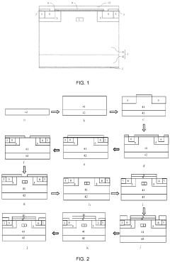
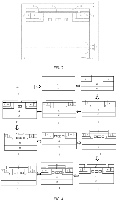
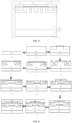
01 SiC MOSFET Structure and Fabrication
Silicon Carbide (SiC) MOSFETs feature unique structural designs that enhance performance characteristics. These devices typically incorporate specialized gate structures, channel formations, and doping profiles that contribute to their superior electrical properties. Advanced fabrication techniques, including epitaxial growth methods and specialized annealing processes, are employed to create high-quality SiC interfaces and reduce defect densities, which are critical for optimal device performance.- SiC MOSFET structure optimization: Silicon Carbide (SiC) MOSFET performance can be enhanced through structural optimizations. These include improved gate designs, channel engineering, and novel device architectures that reduce parasitic resistances and capacitances. Such structural improvements lead to better switching characteristics, reduced on-resistance, and higher breakdown voltages, which are critical for high-power applications.
- Thermal management techniques: Effective thermal management is crucial for SiC MOSFET performance. Various techniques including advanced packaging solutions, heat dissipation structures, and thermal interface materials help maintain optimal operating temperatures. These approaches prevent performance degradation under high-temperature conditions and extend device lifetime, allowing SiC MOSFETs to fully utilize their inherent high-temperature operation capability.
- Interface quality improvement: The SiC/oxide interface quality significantly impacts MOSFET performance. Techniques for reducing interface traps and defects include specialized oxidation processes, post-oxidation annealing treatments, and interface passivation methods. Improving this interface leads to enhanced channel mobility, reduced threshold voltage instability, and more reliable device operation under various stress conditions.
- Driving circuit optimization: Specialized gate driving circuits are essential for maximizing SiC MOSFET performance. These circuits address the unique switching characteristics of SiC devices, including faster switching speeds and different gate voltage requirements compared to silicon counterparts. Optimized drivers reduce switching losses, prevent parasitic turn-on, and enable the full utilization of SiC MOSFET high-frequency operation capabilities.
- Reliability enhancement methods: Enhancing SiC MOSFET reliability involves addressing specific failure mechanisms such as threshold voltage instability, body diode degradation, and gate oxide reliability. Various techniques including specialized bias stress testing, improved passivation layers, and robust protection circuits help ensure stable long-term performance. These methods are particularly important for applications requiring high reliability such as automotive, aerospace, and industrial power systems.
02 Thermal Performance and Reliability
SiC MOSFETs demonstrate exceptional thermal performance characteristics, allowing operation at higher temperatures compared to silicon-based devices. Their superior thermal conductivity enables more efficient heat dissipation, reducing thermal resistance and improving overall reliability. Various packaging technologies and thermal management solutions have been developed specifically for SiC MOSFETs to maximize their temperature handling capabilities and ensure long-term operational stability under demanding conditions.Expand Specific Solutions03 Switching Characteristics and Efficiency
The switching performance of SiC MOSFETs is characterized by faster switching speeds, lower switching losses, and reduced parasitic capacitances compared to conventional silicon devices. These properties enable higher frequency operation and improved efficiency in power conversion applications. Gate driver designs and circuit topologies have been optimized specifically for SiC MOSFETs to fully leverage their switching capabilities while mitigating challenges such as voltage overshoots and electromagnetic interference.Expand Specific Solutions04 Interface Quality and Channel Mobility
The performance of SiC MOSFETs is significantly influenced by the quality of the SiC/oxide interface and channel mobility characteristics. Various techniques have been developed to improve interface quality, including specialized oxidation processes, post-oxidation annealing treatments, and interface passivation methods. These approaches aim to reduce interface trap densities and enhance channel mobility, which directly impacts key performance parameters such as on-resistance and threshold voltage stability.Expand Specific Solutions05 Application-Specific Optimization
SiC MOSFETs are increasingly being optimized for specific application requirements, including electric vehicles, renewable energy systems, and industrial power supplies. These optimizations involve tailoring device characteristics such as breakdown voltage, on-resistance, and gate charge to meet particular application needs. Advanced modeling and simulation techniques are employed to predict device behavior under various operating conditions, enabling more effective application-specific designs and system integration approaches.Expand Specific Solutions
Leading Manufacturers and Research Institutions in SiC Power Electronics
The SiC MOSFET market is currently in a growth phase, with parasitic inductance emerging as a critical performance factor as switching frequencies increase. The global market is projected to reach $2.5 billion by 2025, driven by electric vehicle adoption and renewable energy applications. Leading semiconductor manufacturers like Infineon Technologies, ROHM, Texas Instruments, and STMicroelectronics have developed advanced packaging techniques and gate driver designs to mitigate parasitic inductance effects. Academic institutions including Xidian University and University of Electronic Science & Technology of China are collaborating with industry players like Mitsubishi Electric and Fuji Electric to advance layout optimization and multi-physics modeling approaches, pushing SiC technology toward higher efficiency and reliability in high-frequency power conversion applications.
ROHM Co., Ltd.
Technical Solution: ROHM has pioneered innovative package designs specifically engineered to minimize parasitic inductance in SiC MOSFET applications. Their SCT3xxx series implements a proprietary trench gate structure that inherently reduces internal gate resistance and improves immunity to parasitic inductance effects. ROHM's research has demonstrated that their optimized packaging can reduce common source inductance by approximately 60% compared to standard TO-247 packages, resulting in switching loss reductions of up to 35%. The company has developed specialized gate driver ICs (such as their BM6112FV series) specifically designed to work with their SiC MOSFETs in high-inductance environments, incorporating features like adjustable slew rate control and active Miller clamp functionality. ROHM's power modules feature direct lead bonding technology that eliminates wire bonds, a significant source of parasitic inductance, reducing the overall module inductance by approximately 40% compared to conventional designs. Their testing has shown that these combined approaches can improve switching efficiency by 15-20% in typical motor drive applications.
Strengths: Comprehensive vertical integration from SiC substrate to module level allows for optimized designs across the entire power conversion chain; specialized packaging technology with extremely low parasitic inductance. Weaknesses: Higher cost compared to some competitors; limited availability of some specialized package options in certain markets.
Infineon Technologies Austria AG
Technical Solution: Infineon has developed advanced SiC MOSFET designs that specifically address parasitic inductance challenges through optimized package designs and chip layouts. Their CoolSiC™ technology incorporates innovative gate driver solutions with optimized switching paths to minimize loop inductances. The company has implemented multi-layer PCB designs with embedded power loops that reduce parasitic inductance by up to 50% compared to conventional layouts. Infineon's power modules feature laminated busbar structures and integrated decoupling capacitors positioned extremely close to the switching devices, effectively minimizing the commutation loop area. Their research has demonstrated that reducing package-related parasitic inductance from 15nH to 5nH can decrease switching losses by approximately 30% while improving EMI performance by up to 15dB in certain frequency ranges.
Strengths: Industry-leading package designs with extremely low parasitic inductance values; comprehensive system-level approach addressing both device and circuit layout optimization. Weaknesses: Premium pricing compared to silicon alternatives; requires specialized design knowledge to fully leverage the low-inductance benefits in end applications.
Key Technical Innovations in Low-Inductance Package Designs
Silicon carbide metal oxide semiconductor field effect transistor device
PatentPendingUS20230387290A1
Innovation
- The silicon carbide metal-oxide-semiconductor field-effect transistor (SiC MOSFET) device is designed with a substrate and epitaxy layer, featuring cell units with specific conductivity types and structures that include Schottky regions, junction field effect regions, well regions, and gate structures, allowing for reduced forward bias voltage, decreased gate electrode capacitance, and enhanced current density through optimized cell configurations and implantation sections.
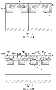
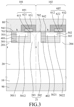
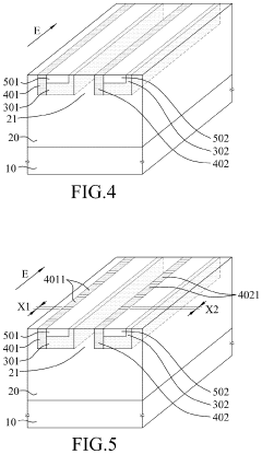
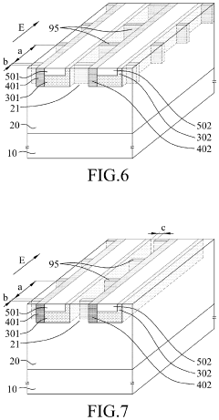
Silicon carbide metal oxide semiconductor field effect transistor and manufacturing method therefor
PatentInactiveEP3813127A1
Innovation
- A silicon carbide metal-oxide-semiconductor field-effect transistor structure is developed, incorporating a second conduction type epitaxial layer, first conduction type well regions, and additional doping regions within the JFET region to reduce gate oxide electric field strength, including a gate oxide layer and passivation protection, with specific doping concentrations and geometries to enhance device performance.
Thermal Management Considerations in SiC MOSFET Applications
Thermal management is a critical aspect of SiC MOSFET implementation that directly impacts how parasitic inductance affects device performance. SiC MOSFETs operate at significantly higher switching frequencies and power densities than traditional silicon devices, generating concentrated heat that must be efficiently dissipated to maintain reliability and performance.
The thermal conductivity of SiC (approximately 3.7 W/cm·K) exceeds that of silicon (1.5 W/cm·K), theoretically enabling better heat dissipation. However, parasitic inductance creates additional switching losses that manifest as heat, complicating thermal management strategies. When parasitic inductance causes voltage overshoots and ringing, the resulting dynamic losses contribute to localized hotspots within the device structure.
Junction temperature management becomes particularly challenging as parasitic inductance increases switching losses by up to 15-20% in poorly designed layouts. Research indicates that for every 10°C rise in junction temperature above recommended operating conditions, SiC MOSFET lifetime may decrease by 30-50%. This temperature sensitivity makes thermal considerations inseparable from parasitic inductance mitigation.
Advanced cooling solutions such as direct liquid cooling, double-sided cooling, and phase-change materials are increasingly necessary to address the thermal challenges exacerbated by parasitic inductance. These solutions must account for the rapid thermal transients characteristic of SiC devices operating with parasitic elements in the circuit.
Thermal interface materials (TIMs) with enhanced thermal conductivity (>5 W/m·K) are essential when managing heat in high-frequency SiC applications where parasitic inductance is present. The selection of appropriate TIMs can reduce thermal resistance by 30-40% compared to conventional materials, helping mitigate the thermal impact of parasitic-induced losses.
Dynamic thermal management systems that respond to temperature fluctuations caused by parasitic-induced switching events are emerging as a critical technology. These systems incorporate temperature sensors with response times under 1ms and adaptive cooling mechanisms that adjust to changing thermal loads during operation.
Computational fluid dynamics (CFD) modeling has become indispensable for predicting thermal behavior in SiC MOSFET systems, allowing engineers to simulate the combined effects of parasitic inductance and thermal constraints before physical implementation. These simulations typically reveal that reducing parasitic inductance by 50% can lower peak junction temperatures by 15-25°C under identical operating conditions.
EMI/EMC Implications of Parasitic Inductance in Power Electronics
Parasitic inductance in power electronics systems significantly impacts electromagnetic interference (EMI) and electromagnetic compatibility (EMC) performance, particularly in high-frequency switching applications using SiC MOSFETs. The rapid switching transitions characteristic of SiC devices (typically 10-100 ns) create high di/dt and dv/dt rates that interact with parasitic inductance to generate substantial electromagnetic noise.
When current through parasitic inductances changes rapidly, voltage spikes (V = L × di/dt) are produced across these inductances. These transients can reach hundreds of volts in poorly designed circuits, creating broadband electromagnetic emissions spanning from hundreds of kHz to hundreds of MHz. Such emissions can propagate through both conducted and radiated paths, potentially interfering with nearby electronic systems.
The common-mode noise pathway is particularly problematic in SiC MOSFET applications. Parasitic inductance in the gate-drive loop can couple with power loop inductance, creating common-mode currents that flow through parasitic capacitances to ground. This mechanism is exacerbated by the higher switching speeds of SiC devices compared to traditional silicon counterparts.
Power loop inductance also contributes significantly to differential-mode noise. The resonance between parasitic inductance and output capacitance of SiC MOSFETs creates oscillatory behavior during switching transitions. These oscillations manifest as "ringing" in voltage and current waveforms, generating spectral content at frequencies typically between 10-500 MHz depending on circuit parameters.
From an EMC compliance perspective, these emissions often challenge regulatory limits established by standards such as CISPR 11, CISPR 22, and FCC Part 15. The higher frequency content associated with SiC MOSFET switching makes traditional EMI filtering approaches less effective, as filter components exhibit degraded performance at higher frequencies due to their own parasitic elements.
Mitigation strategies must address layout optimization to minimize loop areas and critical path inductances. Multi-layer PCBs with dedicated power and ground planes can reduce both loop inductance and common-mode emissions. Advanced packaging technologies like embedded die and integrated power modules also offer significant reductions in parasitic inductance, improving EMI/EMC performance.
Shielding and filtering solutions must be specifically designed for the higher frequency emissions characteristic of SiC MOSFET circuits. Conventional EMI filters designed for silicon IGBT applications often prove inadequate without modification to address higher frequency components. Hybrid filtering approaches combining conventional passive filters with active cancellation techniques show promising results in laboratory testing.
Unlock deeper insights with PatSnap Eureka Quick Research — get a full tech report to explore trends and direct your research. Try now!
Generate Your Research Report Instantly with AI Agent
Supercharge your innovation with PatSnap Eureka AI Agent Platform!