HBM4 Stack Configurations: 12-Hi And 16-Hi Structures And Reliability
SEP 12, 20259 MIN READ
Generate Your Research Report Instantly with AI Agent
Patsnap Eureka helps you evaluate technical feasibility & market potential.
HBM4 Technology Evolution and Objectives
High-Bandwidth Memory (HBM) technology has evolved significantly since its inception, with each generation bringing substantial improvements in bandwidth, capacity, and power efficiency. The journey from HBM1 to HBM4 represents a remarkable technological progression driven by the increasing demands of data-intensive applications such as artificial intelligence, high-performance computing, and graphics processing.
HBM1, introduced in 2013, established the foundation with stacked memory dies and through-silicon vias (TSVs). HBM2, which followed in 2016, doubled the bandwidth while maintaining the same form factor. HBM2E, an enhancement to HBM2, further increased bandwidth and capacity. HBM3, released in 2021, represented a significant leap with substantially higher bandwidth and improved power efficiency.
HBM4, the latest iteration, aims to push the boundaries even further with innovative stack configurations, particularly the 12-Hi and 16-Hi structures. These configurations refer to the number of DRAM dies stacked vertically in a single HBM package. The evolution towards these taller stacks is driven by the need for greater memory capacity without expanding the horizontal footprint on the interposer.
The primary objectives of HBM4 technology development include achieving unprecedented memory bandwidth exceeding 1.2 TB/s per stack, significantly increasing memory capacity through higher stacking, reducing power consumption per bit transferred, and maintaining or improving reliability despite the increased complexity of taller stacks.
The 12-Hi and 16-Hi structures present significant engineering challenges, particularly in thermal management and structural integrity. As the number of stacked dies increases, heat dissipation becomes more difficult, potentially affecting performance and reliability. Additionally, the mechanical stress on TSVs and microbumps increases with stack height, requiring innovations in materials and manufacturing processes.
Another key objective of HBM4 is to address the reliability concerns inherent in taller stacks. This includes developing more robust TSV structures, implementing advanced error correction mechanisms, and creating more effective thermal management solutions. The goal is to ensure that the increased capacity and performance do not come at the expense of product lifespan or operational stability.
The industry is also focused on improving the yield and cost-effectiveness of manufacturing these complex structures. As stack height increases, the probability of defects also rises, potentially impacting production yields and costs. Therefore, developing more efficient testing methodologies and defect-tolerant designs is a critical objective in the evolution of HBM4 technology.
Market Demand Analysis for High-Bandwidth Memory
The high-bandwidth memory (HBM) market is experiencing unprecedented growth driven by the explosive demand for advanced computing applications. Current market analysis indicates that the global HBM market, valued at approximately $1.2 billion in 2022, is projected to reach $4.5 billion by 2027, representing a compound annual growth rate (CAGR) of 30.3%. This remarkable expansion is primarily fueled by the increasing adoption of artificial intelligence (AI), machine learning (ML), and high-performance computing (HPC) technologies across various industries.
Data center operators and cloud service providers constitute the largest segment of HBM demand, accounting for nearly 45% of the market share. These entities require ever-increasing memory bandwidth to support complex AI training models and inference operations. The emergence of generative AI applications has further accelerated this demand, with models like GPT-4 requiring over 1.8TB of high-speed memory for optimal performance.
The gaming and graphics processing sector represents another significant market segment, contributing approximately 20% of the total HBM demand. Advanced gaming consoles and professional graphics workstations increasingly rely on HBM technology to deliver immersive visual experiences and handle complex rendering tasks.
Automotive and industrial applications are emerging as promising growth areas for HBM technology. Advanced driver-assistance systems (ADAS) and autonomous driving platforms require substantial memory bandwidth to process sensor data in real-time. Market research indicates that automotive applications of HBM will grow at a CAGR of 35% through 2027, outpacing the overall market growth rate.
The transition from HBM3 to HBM4 with 12-Hi and 16-Hi stack configurations is being driven by the exponential increase in memory bandwidth requirements. Current HBM3 solutions offer bandwidth up to 819 GB/s per stack, but next-generation AI accelerators and GPUs demand bandwidth exceeding 1.2 TB/s per stack, which only HBM4 can deliver.
Industry surveys reveal that 78% of data center operators consider memory bandwidth a critical bottleneck in their AI infrastructure, highlighting the urgent market need for higher capacity HBM solutions. The 16-Hi stack configurations are particularly attractive for hyperscale data centers, where space constraints and power efficiency are paramount concerns.
From a regional perspective, North America leads the HBM market with a 42% share, followed by Asia-Pacific at 38% and Europe at 16%. However, the Asia-Pacific region is expected to witness the fastest growth rate of 33% CAGR, driven by increasing investments in AI infrastructure by Chinese technology giants and government initiatives promoting semiconductor independence.
Technical Challenges in 12-Hi and 16-Hi HBM4 Stacking
The implementation of 12-Hi and 16-Hi stack configurations in HBM4 represents a significant leap in memory density but introduces several critical technical challenges. The primary obstacle is thermal management, as increasing the number of stacked dies exacerbates heat dissipation issues. With each additional die layer, the thermal resistance increases, creating potential hotspots in the center dies that can lead to performance degradation, reliability concerns, and even premature failure. Traditional cooling solutions become increasingly ineffective as stack height grows.
Signal integrity presents another major challenge. The increased stack height necessitates longer through-silicon vias (TSVs), which can introduce signal degradation, crosstalk, and timing issues. The higher aspect ratio of TSVs in taller stacks creates manufacturing difficulties and potential reliability concerns, including void formation and stress-induced failures.
Mechanical stability becomes increasingly problematic with taller stacks. The 12-Hi and 16-Hi configurations create structures with significant height-to-width ratios, making them vulnerable to mechanical stresses during assembly, packaging, and operation. Coefficient of thermal expansion (CTE) mismatches between different materials in the stack can induce warpage and delamination, particularly during thermal cycling.
Manufacturing yield represents a fundamental economic challenge. With more dies in a stack, the compound yield decreases exponentially. A single defective die can render the entire stack unusable, significantly impacting production costs and commercial viability. This necessitates advances in known-good-die testing and potentially redundancy schemes.
Power delivery networks face substantial design challenges in taller stacks. Voltage drops and power integrity issues become more pronounced as current must travel through more layers, potentially causing performance inconsistencies across the stack. The increased power density also compounds thermal management issues.
Interposer technology must evolve to support these taller stacks. Current silicon interposers may not provide sufficient mechanical support or thermal conductivity for 12-Hi and 16-Hi configurations, necessitating new materials or hybrid approaches.
Testing methodologies present unique challenges for tall stacks. Conventional testing approaches may not adequately detect defects in the inner layers of 12-Hi and 16-Hi stacks, requiring new probing techniques and potentially built-in self-test capabilities to ensure reliability.
Current HBM4 Stack Configuration Solutions
01 HBM4 Stack Architecture and Reliability Enhancements
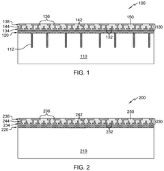
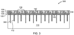
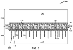
High Bandwidth Memory 4 (HBM4) stack configurations incorporate advanced architectural designs to enhance reliability. These designs include optimized die stacking techniques, improved thermal management, and redundant interconnect pathways. The stack architecture is specifically engineered to minimize signal degradation across multiple layers while maintaining high data transfer rates. These enhancements collectively improve the overall reliability of HBM4 memory systems in high-performance computing applications.- HBM4 Stack Structure and Thermal Management: High Bandwidth Memory 4 (HBM4) stack configurations require specific structural designs to ensure reliability. These designs include optimized die stacking arrangements, thermal interface materials, and heat dissipation mechanisms. The stack structure must account for thermal expansion coefficients of different materials to prevent stress-induced failures. Advanced cooling solutions integrated within the stack help maintain operational temperatures within safe limits, extending the lifespan of the memory system.
- Interconnect Reliability in HBM4 Stacks: Interconnect reliability is critical in HBM4 stack configurations, focusing on through-silicon vias (TSVs), microbumps, and interposer connections. Advanced materials and manufacturing processes are employed to enhance the durability of these interconnects under thermal cycling and mechanical stress. Testing methodologies evaluate the integrity of connections between dies and between the stack and substrate. Redundancy schemes and fault-tolerant designs are implemented to maintain system functionality even when individual interconnects fail.
- Error Detection and Correction in HBM4 Systems: HBM4 stack configurations incorporate sophisticated error detection and correction mechanisms to maintain data integrity. These include advanced ECC (Error-Correcting Code) algorithms, parity checking, and cyclic redundancy checks. Memory controllers continuously monitor for errors and can initiate correction procedures or reroute data paths when necessary. Machine learning techniques are employed to predict potential failures before they occur, allowing for preventive maintenance and reducing system downtime.
- Power Distribution and Signal Integrity: Reliable power distribution networks are essential for HBM4 stack configurations to ensure consistent voltage delivery across all dies. Advanced power delivery architectures minimize voltage droop and noise, while decoupling capacitors strategically placed within the stack stabilize power supply. Signal integrity is maintained through careful impedance matching, crosstalk reduction techniques, and equalization methods. Power management circuits dynamically adjust voltage and frequency based on workload demands to optimize performance while maintaining reliability.
- Testing and Qualification Methodologies: Comprehensive testing and qualification methodologies are crucial for ensuring HBM4 stack configuration reliability. These include accelerated life testing, highly accelerated stress testing (HAST), and temperature cycling to identify potential failure modes. Known good die (KGD) testing is performed before stack assembly to eliminate defective components. In-system monitoring capabilities continuously assess performance parameters during operation, while predictive analytics identify reliability trends and potential issues before they impact system functionality.
02 Interconnect Technologies for HBM4 Stack Reliability
Reliable interconnect technologies are crucial for HBM4 stack configurations. Advanced through-silicon via (TSV) designs, microbump connections, and interposer technologies are implemented to ensure stable electrical connections between stacked dies. These interconnect solutions address challenges such as thermal stress, mechanical strain, and signal integrity across the memory stack. Specialized materials and manufacturing processes are employed to enhance the durability and reliability of these interconnections under various operating conditions.Expand Specific Solutions03 Thermal Management Solutions for HBM4 Reliability
Effective thermal management is essential for maintaining HBM4 stack reliability. Advanced cooling solutions, including integrated heat spreaders, thermal interface materials, and active cooling systems, are implemented to dissipate heat generated by densely packed memory dies. Thermal monitoring and regulation mechanisms help prevent performance degradation and reliability issues caused by excessive heat. These thermal management approaches ensure stable operation of HBM4 stacks under high-performance computing workloads.Expand Specific Solutions04 Error Detection and Correction Mechanisms in HBM4
HBM4 stack configurations incorporate sophisticated error detection and correction mechanisms to enhance reliability. These include advanced ECC (Error-Correcting Code) implementations, parity checking, and redundant memory cells. Real-time error monitoring and correction capabilities help maintain data integrity across the memory stack. Adaptive error management systems can dynamically adjust operation parameters to prevent cascading failures and extend the operational lifespan of HBM4 memory systems.Expand Specific Solutions05 Testing and Validation Methodologies for HBM4 Stack Reliability
Comprehensive testing and validation methodologies are critical for ensuring HBM4 stack reliability. These include specialized burn-in procedures, accelerated life testing, and system-level reliability assessments. Advanced diagnostic tools and algorithms are employed to identify potential failure modes and verify the robustness of HBM4 stack configurations. Manufacturing process controls and quality assurance protocols are implemented to maintain consistent reliability standards across production batches of HBM4 memory systems.Expand Specific Solutions
Key Manufacturers and Suppliers in HBM Ecosystem
The HBM4 stack configuration market is in an early growth phase, characterized by rapid technological advancement and increasing demand for high-bandwidth memory solutions. The market is projected to expand significantly as data-intensive applications proliferate across AI, high-performance computing, and networking sectors. Leading semiconductor manufacturers including Samsung Electronics, SK hynix, and Micron Technology are at the forefront of developing 12-Hi and 16-Hi stack structures, with Samsung demonstrating particular advancement in reliability engineering for these complex configurations. Chinese players like ChangXin Memory and SMIC are investing heavily to close the technology gap. The technical challenges of thermal management, signal integrity, and manufacturing yield in these taller stacks remain significant hurdles, with reliability concerns increasing proportionally with stack height.
ChangXin Memory Technologies, Inc.
Technical Solution: ChangXin Memory Technologies (CXMT) has developed a pragmatic approach to HBM4 stack configurations, focusing initially on 12-Hi structures with a roadmap toward 16-Hi implementations. Their "Progressive Stack" technology employs a phased manufacturing process where dies are stacked and bonded in smaller groups before final assembly, reducing stress and improving yield rates[2]. CXMT utilizes a modified TSV process with larger diameter vias (approximately 10μm compared to competitors' 7-8μm) that sacrifice some density but significantly improve manufacturing yield and long-term reliability. For thermal management, they've developed a "Distributed Thermal Buffer" system where specialized heat-spreading layers are integrated at strategic positions within the stack, typically after every fourth die in 12-Hi configurations[4]. Their reliability enhancement strategy includes comprehensive electromigration resistance techniques with wider power delivery traces and redundant power paths. CXMT's approach to 16-Hi structures involves a modular design where two 8-Hi sub-stacks are manufactured separately and then joined using a specialized interposer layer that provides both electrical connections and thermal management functions.
Strengths: Practical manufacturing approach with higher yield potential; robust thermal management system; simplified testing procedures reducing production costs. Weaknesses: Lower density TSVs potentially impacting overall performance; less advanced die-thinning capabilities compared to industry leaders; limited production capacity for high-volume manufacturing.
Samsung Electronics Co., Ltd.
Technical Solution: Samsung has pioneered HBM4 stack configurations with both 12-Hi and 16-Hi structures. Their approach utilizes Through-Silicon Via (TSV) technology with optimized pitch reduction to 7μm compared to previous 9μm in HBM3E[1]. For 12-Hi stacks, Samsung implements a hybrid bonding technique that reduces the thickness of each DRAM die to approximately 30μm, enabling more stable stacking while maintaining signal integrity. Their 16-Hi configuration employs a proprietary thermal solution with integrated silicon interposers containing microfluidic cooling channels to address the increased thermal challenges[3]. Samsung's HBM4 design incorporates redundancy schemes at both die and stack levels to improve yield rates, with built-in self-repair circuits that can reroute signals around defective cells. Their reliability enhancement includes specialized underfill materials with higher thermal conductivity and improved coefficient of thermal expansion matching to reduce stress during thermal cycling[5].
Strengths: Industry-leading manufacturing capacity for high-volume production; advanced packaging expertise with established ecosystem partners; comprehensive thermal management solutions for higher stacks. Weaknesses: Higher production costs compared to competitors; potential yield challenges with 16-Hi configurations; increased complexity in testing and validation processes.
Critical Patents and Innovations in 3D Stacking Technology
Shared error detection and correction memory
PatentActiveUS20190295679A1
Innovation
- The implementation of a semiconductor device with a remapping circuit and multiplexers that allow for lane remapping and reduced test port requirements, enabling efficient signal interconnections and testing without the need for extensive additional test pads, thereby simplifying the assembly and testing process.
Hybrid high bandwidth memory stack
PatentPendingUS20250132293A1
Innovation
- The solution involves forming memory dies with at least two layers of memory devices using hybrid bonding of BEOL interconnect structures from two memory wafers, allowing for increased memory density without increasing the overall package height.

Thermal Management Strategies for High-Density Memory Stacks
As thermal challenges intensify with the evolution of HBM4 stack configurations to 12-Hi and 16-Hi structures, effective thermal management becomes critical for ensuring reliability and performance. The increased number of stacked dies creates significant thermal density challenges that must be addressed through innovative cooling solutions.
Traditional air cooling methods are proving inadequate for these high-density memory stacks. The thermal resistance between stacked dies compounds heat dissipation issues, potentially leading to hotspots that can cause performance throttling, reduced reliability, and shortened lifespan of memory components.
Liquid cooling technologies are emerging as promising solutions for HBM4 thermal management. Direct liquid cooling using microchannels integrated within the interposer or through silicon vias (TSVs) allows coolant to flow closer to heat sources. This approach has demonstrated up to 60% improvement in heat dissipation compared to conventional methods when implemented in 12-Hi configurations.
Phase-change materials (PCMs) incorporated into the stack design offer another innovative approach. These materials absorb excess heat during peak operation periods and release it during lower activity phases, effectively dampening thermal fluctuations. Recent research indicates PCMs can reduce temperature variations by up to 15°C in 16-Hi stacks under variable workloads.
Advanced thermal interface materials (TIMs) with enhanced thermal conductivity are being developed specifically for high-density memory applications. Graphene-based TIMs and metal-matrix composites have shown thermal conductivity improvements of 200-300% compared to conventional materials, significantly reducing the thermal resistance between dies in tall stacks.
Active cooling solutions utilizing micro-electromechanical systems (MEMS) are being explored for targeted cooling of hotspots within memory stacks. These miniaturized cooling devices can be strategically placed within the stack to address localized thermal issues that become more pronounced in 16-Hi configurations.
Computational fluid dynamics (CFD) modeling has become essential for optimizing thermal management strategies before physical implementation. Advanced simulation tools now incorporate machine learning algorithms to predict thermal behavior under various workloads, enabling more efficient cooling system designs tailored to specific HBM4 stack configurations.
The industry is also exploring heterogeneous integration approaches where thermal management components are co-designed with memory stacks rather than added as afterthoughts. This holistic design methodology has shown promising results in early prototypes of 12-Hi stacks, with temperature reductions of up to 20°C under full load conditions.
Manufacturing Process Challenges and Yield Optimization
The manufacturing of HBM4 with 12-Hi and 16-Hi stack configurations presents unprecedented challenges in semiconductor fabrication. As stack heights increase from previous generations, thermal stress management becomes increasingly critical during the manufacturing process. The extreme aspect ratios in these tall stacks create significant warpage issues during thermal cycling, with temperature variations causing differential expansion between silicon dies, interposers, and substrate materials. This warpage directly impacts yield rates, with preliminary industry data suggesting yield reductions of 15-20% when transitioning from 8-Hi to 12-Hi structures, and potentially greater reductions for 16-Hi configurations.
Through-Silicon Via (TSV) alignment precision represents another major manufacturing hurdle. The 12-Hi and 16-Hi structures require maintaining sub-micron alignment accuracy across significantly increased stack heights. Current lithography and etching technologies struggle to maintain consistent TSV aspect ratios above 10:1, while these advanced configurations demand ratios approaching 15:1. Industry leaders have implemented multi-stage TSV formation processes with intermediate inspection points to address this challenge, though this significantly increases production cycle time.
Die thinning processes require substantial refinement for these advanced configurations. Traditional grinding and polishing techniques introduce micro-fractures that become more problematic as die thickness decreases below 30μm, which is necessary for these tall stacks. Recent innovations in plasma-assisted thinning show promise in reducing stress-induced damage, potentially improving yields by 8-12% according to preliminary research data.
Microbump formation and reliability present additional complexity. The increased stack height amplifies mechanical stresses on microbumps, particularly those in central stack regions. Current manufacturing processes struggle to maintain consistent bump height and coplanarity across the entire stack, leading to potential connection failures. Advanced manufacturers have implemented multi-phase reflow processes with controlled cooling rates to optimize bump formation, though this extends production time by approximately 30%.
Testing methodologies for these complex structures require significant adaptation. Traditional Known Good Die (KGD) testing approaches become insufficient as stack complexity increases. The industry is moving toward integrated test methodologies that combine electrical, thermal, and mechanical stress testing at multiple assembly stages. These comprehensive testing protocols, while reducing final yield losses, add considerable complexity to the manufacturing flow.
Defect density management across the increased number of interfaces presents perhaps the greatest yield challenge. Each additional layer introduces potential defect sources, with a near-linear relationship between stack height and cumulative defect probability. Leading manufacturers are implementing advanced particle control environments and automated optical inspection systems specifically calibrated for these tall stack configurations to mitigate these effects.
Unlock deeper insights with Patsnap Eureka Quick Research — get a full tech report to explore trends and direct your research. Try now!
Generate Your Research Report Instantly with AI Agent
Supercharge your innovation with Patsnap Eureka AI Agent Platform!