How Does Chiplet Integration Impact Electronics Regulation Compliance
OCT 15, 20259 MIN READ
Generate Your Research Report Instantly with AI Agent
Patsnap Eureka helps you evaluate technical feasibility & market potential.
Chiplet Integration Technology Background and Objectives
Chiplet integration represents a paradigm shift in semiconductor design and manufacturing, evolving from the traditional monolithic system-on-chip (SoC) approach to a more modular architecture. This technological evolution began in the early 2010s as semiconductor manufacturers faced increasing challenges with Moore's Law, particularly regarding yield, performance, and cost considerations at advanced process nodes. The fundamental concept involves disaggregating complex SoCs into smaller functional blocks (chiplets) that can be manufactured separately and then integrated using advanced packaging technologies.
The historical trajectory of chiplet technology shows significant acceleration since 2017, with companies like AMD pioneering commercial implementation through their Infinity Fabric interconnect in Ryzen processors. Intel followed with their Embedded Multi-die Interconnect Bridge (EMIB) and Foveros technologies, while TSMC developed their Integrated Fan-Out (InFO) and System on Integrated Chips (SoIC) solutions. This evolution represents a response to the physical limitations of traditional semiconductor scaling and the economic challenges of advanced node manufacturing.
From a regulatory compliance perspective, chiplet integration introduces novel considerations across multiple domains. Traditional compliance frameworks were developed primarily for monolithic designs, creating potential gaps in addressing the unique characteristics of multi-die packages. The integration of heterogeneous components manufactured at different process nodes, potentially by different vendors, introduces new variables in electromagnetic compatibility (EMC), thermal management, and reliability assessment.
The primary technical objectives for chiplet integration in relation to regulatory compliance include developing standardized testing methodologies specifically adapted for multi-die packages, establishing clear responsibility frameworks for compliance when multiple vendors contribute to a single product, and creating predictive models that can accurately assess compliance risks during the design phase rather than post-integration.
Industry consortia such as the Universal Chiplet Interconnect Express (UCIe) and JEDEC have begun addressing these challenges by working toward standardization of chiplet interfaces and testing protocols. However, significant work remains to fully harmonize chiplet technology with global regulatory frameworks including FCC, CE, UL, and other regional certification requirements.
The convergence of chiplet technology with emerging applications in artificial intelligence, high-performance computing, and telecommunications infrastructure further amplifies the importance of resolving these regulatory challenges. As chiplet integration becomes more prevalent across consumer electronics, medical devices, automotive systems, and critical infrastructure, the need for comprehensive compliance frameworks becomes increasingly urgent.
Market Demand Analysis for Chiplet-Based Electronics
The global market for chiplet-based electronics is experiencing unprecedented growth, driven by the increasing demand for high-performance computing solutions across multiple sectors. Current market projections indicate that the chiplet technology market is expected to grow at a compound annual growth rate of 40% through 2027, reaching approximately $5.8 billion by that year. This remarkable growth trajectory is primarily fueled by the semiconductor industry's shift away from traditional monolithic designs toward more modular and efficient architectures.
Data center operators represent the largest current market segment for chiplet technology, as they continuously seek solutions to address escalating computational demands while managing power consumption and thermal constraints. The hyperscale cloud service providers are particularly aggressive in adopting chiplet-based solutions, with major players like AWS, Google Cloud, and Microsoft Azure investing heavily in this technology to support their AI and high-performance computing offerings.
Consumer electronics manufacturers constitute another significant market segment, with smartphone and laptop producers exploring chiplet integration to deliver enhanced performance within strict power and space limitations. Market research indicates that approximately 30% of premium smartphones could incorporate some form of chiplet technology by 2025, representing a substantial market opportunity.
The automotive sector is emerging as a rapidly growing market for chiplet-based electronics, particularly for advanced driver assistance systems (ADAS) and autonomous driving platforms. The need for high-performance, energy-efficient computing in vehicles is driving adoption, with the automotive chiplet market segment projected to grow at 45% annually through 2026.
Industrial automation and edge computing applications are also creating substantial demand for chiplet technology. These sectors require specialized processing capabilities with optimized power profiles, making chiplet-based solutions increasingly attractive. Market analysis shows that industrial applications could account for 15% of the total chiplet market by 2025.
From a geographic perspective, North America currently leads in chiplet technology adoption, followed closely by East Asia. However, the fastest growth is expected in the Asia-Pacific region, where major semiconductor manufacturers are rapidly expanding their chiplet production capabilities to meet increasing demand.
The market is also being shaped by regulatory considerations, as different regions implement varying standards for electronic devices. This regulatory landscape is creating both challenges and opportunities for chiplet-based electronics, as manufacturers must navigate compliance requirements while leveraging the flexibility that chiplet architecture provides to meet regional specifications efficiently.
Current Regulatory Challenges for Chiplet Integration
Chiplet integration presents significant challenges for regulatory compliance in the electronics industry. The transition from monolithic System-on-Chip (SoC) designs to disaggregated chiplet architectures fundamentally alters how electronic products must be evaluated against established regulatory frameworks. Current regulations were largely developed for traditional integrated circuit paradigms, creating a misalignment with chiplet-based systems that feature multiple die from potentially different manufacturers interconnected within a single package.
Electromagnetic compatibility (EMC) regulations pose particular difficulties as chiplet designs introduce new interference patterns and emission profiles. The high-speed interconnects between chiplets create unique electromagnetic emission signatures that may not be adequately addressed by existing test methodologies. Regulatory bodies such as the FCC in the United States and ETSI in Europe have yet to develop specific testing protocols for multi-die packages, leaving manufacturers to interpret how existing standards should apply.
Thermal management compliance represents another significant challenge. The concentrated power density in chiplet designs, particularly at die-to-die interfaces, creates thermal profiles that differ substantially from monolithic designs. Current thermal testing standards may not adequately capture the complex thermal interactions between multiple chiplets, potentially leading to compliance gaps or overly conservative designs that sacrifice performance unnecessarily.
Supply chain security and traceability requirements become exponentially more complex with chiplet integration. When components from multiple vendors are combined into a single package, establishing a secure chain of custody and verifying the provenance of each element presents regulatory challenges. This is particularly problematic for products destined for government, defense, or critical infrastructure applications where security certifications are mandatory.
Product lifecycle management regulations also face disruption from chiplet technology. End-of-life considerations, repair rights legislation, and electronic waste directives must now account for packages containing multiple semiconductor technologies with different lifespans and recyclability profiles. The modular nature of chiplets theoretically enables more sustainable practices, but current regulations lack frameworks to properly incentivize or standardize such approaches.
International regulatory harmonization presents perhaps the most pressing challenge. Different regions have developed varying approaches to chiplet-related compliance issues, creating a fragmented regulatory landscape. Companies deploying chiplet-based products globally must navigate inconsistent requirements across jurisdictions, increasing compliance costs and potentially limiting innovation. The absence of standardized testing methodologies specifically designed for chiplet architectures further complicates cross-border certification efforts.
Current Compliance Solutions for Chiplet-Based Systems
01 Regulatory compliance frameworks for chiplet integration
Regulatory frameworks govern the integration of chiplets in semiconductor manufacturing, ensuring that the final products meet industry standards and legal requirements. These frameworks include specifications for electrical safety, electromagnetic compatibility, and environmental compliance. Companies must navigate these regulations when designing and manufacturing chiplet-based systems to ensure market acceptance and avoid legal penalties.- Regulatory compliance frameworks for chiplet integration: Regulatory frameworks govern the integration of chiplets in semiconductor manufacturing, ensuring that the final products meet industry standards and legal requirements. These frameworks include specifications for electrical safety, electromagnetic compatibility, and thermal management. Compliance with these regulations is essential for chiplet-based products to be marketed globally, as different regions may have varying requirements that need to be addressed during the design and manufacturing phases.
- Testing and certification protocols for chiplet-based systems: Specific testing and certification protocols are required to ensure chiplet-based systems comply with regulatory standards. These protocols involve rigorous testing of interconnects, power delivery, signal integrity, and thermal performance. Certification processes may include third-party validation and documentation of compliance with standards such as ISO, IEC, or regional requirements. Manufacturers must implement these protocols throughout the development cycle to avoid costly redesigns and ensure market acceptance.
- Intellectual property management in chiplet ecosystems: Managing intellectual property rights is crucial in chiplet integration, as multiple vendors may contribute different chiplets to a single system. This includes establishing clear licensing agreements, patent pools, and standardized interfaces that allow for interoperability while protecting proprietary technologies. Companies must navigate complex IP landscapes to ensure that their chiplet implementations do not infringe on existing patents while maintaining competitive advantages through their own IP portfolios.
- Security and data protection compliance for chiplet architectures: Security and data protection are critical aspects of chiplet integration compliance, particularly for applications in sensitive sectors like finance, healthcare, and defense. Chiplet architectures must implement security features such as secure boot, encryption, and hardware root of trust to protect against vulnerabilities that could arise from the disaggregated nature of chiplet designs. Compliance with data protection regulations like GDPR or HIPAA may require specific security implementations at the chiplet interface level.
- Environmental and sustainability regulations for chiplet manufacturing: Environmental and sustainability regulations impact chiplet manufacturing processes, requiring compliance with standards for hazardous substance restrictions, energy efficiency, and end-of-life recycling. Manufacturers must adhere to regulations such as RoHS, REACH, and energy efficiency standards while documenting the environmental impact of their chiplet production. The modular nature of chiplets can potentially offer advantages in terms of resource efficiency and reduced electronic waste, but manufacturers must ensure their processes align with evolving environmental regulations.
02 Thermal management compliance in chiplet designs
Thermal management is a critical aspect of chiplet integration that must comply with specific regulations. This includes ensuring proper heat dissipation, maintaining safe operating temperatures, and implementing cooling solutions that meet industry standards. Compliance in this area is essential to prevent thermal-related failures and ensure the reliability and longevity of chiplet-based systems.Expand Specific Solutions03 Data security and privacy compliance for integrated chiplets
As chiplet integration often involves components that process sensitive data, compliance with data security and privacy regulations is essential. This includes implementing secure communication protocols between chiplets, ensuring data encryption, and protecting against unauthorized access. Manufacturers must adhere to various international standards and regulations regarding data protection when designing chiplet-based systems.Expand Specific Solutions04 Interoperability standards and certification for chiplet integration
Chiplet integration requires adherence to interoperability standards to ensure that components from different manufacturers can work together seamlessly. This includes compliance with interface specifications, signal integrity requirements, and power delivery standards. Certification processes verify that integrated chiplet solutions meet these standards, providing assurance to customers and regulatory bodies about the compatibility and reliability of the final product.Expand Specific Solutions05 Environmental and sustainability compliance in chiplet manufacturing
Environmental regulations impact chiplet integration, requiring manufacturers to consider sustainability aspects throughout the product lifecycle. This includes compliance with restrictions on hazardous substances, energy efficiency requirements, and end-of-life recycling considerations. Manufacturers must document their compliance with these regulations and may need to obtain specific certifications to sell their chiplet-based products in certain markets.Expand Specific Solutions
Key Industry Players in Chiplet Integration
Chiplet integration is reshaping electronics regulation compliance in a rapidly evolving market currently transitioning from early adoption to mainstream implementation. The global chiplet market is experiencing significant growth, projected to reach substantial scale as major semiconductor players invest heavily in this technology. From a technical maturity perspective, industry leaders like TSMC, Intel, and Samsung are advancing chiplet architectures with varying approaches to integration and standardization. Companies including AMD, Marvell, and MediaTek are implementing chiplet designs in commercial products, while Texas Instruments and NXP focus on specialized applications requiring stringent compliance. Regulatory challenges center around thermal management, electromagnetic compatibility, and cross-border data security, with companies like IBM and Infineon developing solutions to address these compliance hurdles while maintaining the performance benefits of disaggregated chip designs.
Taiwan Semiconductor Manufacturing Co., Ltd.
Technical Solution: TSMC addresses chiplet integration compliance through their Integrated Fan-Out (InFO) and System on Integrated Chips (SoIC) technologies. Their approach includes specialized substrate designs that incorporate EMI shielding directly into the package architecture. TSMC has developed advanced simulation tools that model electromagnetic interactions between chiplets at the package level, allowing designers to identify and mitigate potential compliance issues before manufacturing. Their SoIC technology uses extremely fine-pitch connections between chiplets (less than 10 microns), which inherently reduces EMI radiation compared to traditional package-level interconnects. TSMC also implements specialized power integrity solutions for chiplet designs, including dedicated power delivery networks for each chiplet to minimize noise coupling. Their manufacturing processes include specialized materials with enhanced EMI absorption properties integrated into the package substrate, helping customers meet stringent regulatory requirements across different jurisdictions[2][4].
Strengths: TSMC's advanced packaging technologies offer industry-leading density and performance while maintaining compliance. Their extensive experience as a foundry partner provides deep insights into compliance challenges across diverse applications. Weaknesses: As primarily a manufacturing partner, TSMC's compliance solutions may require significant customer expertise to implement effectively, and their advanced packaging technologies often come at premium price points.
Intel Corp.
Technical Solution: Intel's approach to chiplet integration compliance focuses on their Advanced Interface Bus (AIB) and Embedded Multi-die Interconnect Bridge (EMIB) technologies. Their EMIB technology enables high-density connections between chiplets without requiring expensive silicon interposers, reducing electromagnetic interference (EMI) issues common in traditional multi-chip packages. Intel has developed specific design methodologies to address electromagnetic compatibility (EMC) challenges in their chiplet architectures, including specialized power delivery networks that minimize noise coupling between dies. Their Foveros 3D packaging technology incorporates EMI shielding layers between stacked dies to ensure regulatory compliance while maintaining high performance. Intel also implements comprehensive testing protocols specifically designed for chiplet-based systems, including inter-die crosstalk analysis and system-level EMC pre-compliance testing to identify potential regulatory issues early in the design cycle[1][3].
Strengths: Intel's mature EMIB and Foveros technologies provide proven compliance solutions with established testing methodologies. Their vertical integration allows for comprehensive control over the entire compliance process. Weaknesses: Their proprietary interconnect technologies may create vendor lock-in, and their compliance solutions often require specialized tools and expertise that may not be accessible to smaller manufacturers.
Critical Patents and Standards for Chiplet Regulation
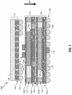
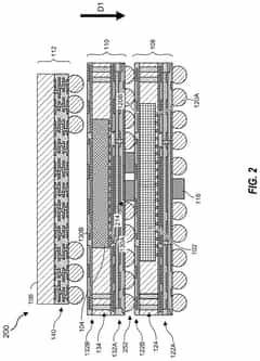
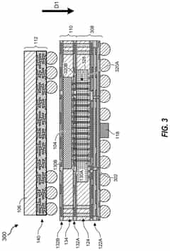
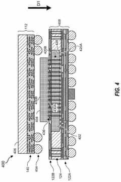
3D chiplet integration using fan-out wafer-level packaging
PatentPendingUS20240274587A1
Innovation
- The use of fan-out wafer-level packaging and three-dimensional packaging techniques for combining semiconductor chips and embedded memory in configurations such as face-to-back, back-to-back, and face-to-face orientations, enabling direct connections between chiplets and reducing assembly package sizes and manufacturing complexity.
Supply Chain Security for Chiplets
PatentPendingUS20250155500A1
Innovation
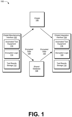
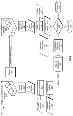
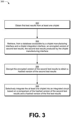
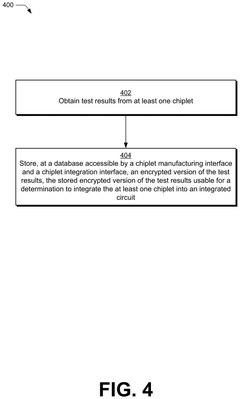
- A system is implemented where a chiplet manufacturing interface tests each chiplet, records the test results securely, and encrypts them using a public-private key pair. These encrypted test results are stored in a shared database accessible by the chiplet integration interface, which decrypts and compares them with its own test results to verify the chiplet's trustworthiness before integration.
Cross-Border Regulatory Framework Analysis
The global regulatory landscape for chiplet-based electronics presents a complex matrix of compliance requirements that vary significantly across jurisdictions. In the United States, the Federal Communications Commission (FCC) has begun adapting its electromagnetic compatibility (EMC) testing protocols to address the unique interference patterns generated by multi-die architectures. Meanwhile, the European Union's approach under the Radio Equipment Directive (RED) and Electromagnetic Compatibility Directive requires comprehensive documentation of each chiplet component, creating additional verification burdens for manufacturers utilizing dies from multiple sources.
Asian regulatory frameworks demonstrate notable divergence in their treatment of chiplet technology. Japan's Ministry of Internal Affairs and Communications has pioneered a "system-level certification" approach that evaluates the integrated package rather than individual components. In contrast, China's regulatory bodies maintain stricter component-level scrutiny through the China Compulsory Certification (CCC) system, requiring detailed technical documentation for each chiplet regardless of its integration context.
The fragmentation of international standards creates significant challenges for global supply chains. Companies must navigate approximately 15-20 different national certification processes when deploying chiplet-based products across major markets. This regulatory complexity has prompted industry consortia such as the Universal Chiplet Interconnect Express (UCIe) to engage with international standards bodies to develop harmonized compliance frameworks that recognize the modular nature of chiplet technology.
Data security regulations introduce another layer of cross-border complexity. The heterogeneous integration of chiplets from different manufacturers raises novel questions about data protection compliance, particularly when processing components cross jurisdictional boundaries with different data sovereignty requirements. The EU's General Data Protection Regulation (GDPR) and China's Personal Information Protection Law impose different obligations regarding hardware security features that must be addressed during the design phase.
Export control regulations represent perhaps the most significant cross-border challenge for chiplet technology. The United States' Export Administration Regulations (EAR) and International Traffic in Arms Regulations (ITAR) impose restrictions on advanced semiconductor technologies that may affect certain chiplet designs. Similarly, the Wassenaar Arrangement's dual-use technology controls create additional compliance requirements for international chiplet supply chains, particularly for high-performance computing applications.
Industry stakeholders are increasingly advocating for regulatory mutual recognition agreements specific to chiplet technology. The Semiconductor Industry Association has proposed a "Chiplet Passport" framework that would standardize technical documentation requirements across borders, potentially reducing compliance costs by an estimated 30-40% while maintaining regulatory oversight.
EMI/EMC Considerations for Multi-Die Systems
Chiplet integration introduces significant challenges in electromagnetic interference (EMI) and electromagnetic compatibility (EMC) compliance due to the complex interconnect structures between multiple dies. Traditional single-die systems typically contain EMI/EMC issues within a single package, but chiplet architectures create new pathways for electromagnetic radiation and susceptibility that must be carefully managed.
The dense interconnect networks between chiplets, particularly high-speed interfaces like UCIe (Universal Chiplet Interconnect Express), can act as unintentional antennas that radiate electromagnetic energy. These emissions may interfere with neighboring components or violate regulatory standards if not properly controlled. Testing has shown that inter-chiplet connections operating at frequencies above 2 GHz are particularly problematic, with potential emissions exceeding FCC Class B limits by 3-6 dB without proper mitigation.
Power delivery networks in multi-die systems present another EMI/EMC challenge. The distributed nature of power consumption across multiple chiplets creates complex current paths that can generate electromagnetic noise. Voltage fluctuations between chiplets operating at different power states can induce transient currents that manifest as broadband EMI, particularly in the 30-300 MHz range where many regulatory limits are most stringent.
Shielding strategies for chiplet-based designs require rethinking traditional approaches. While conventional systems might employ package-level shields, chiplet architectures benefit from more granular shielding between dies. Advanced techniques include embedded Faraday cages within the interposer and selective metallization patterns that create electromagnetic barriers between sensitive analog chiplets and noisy digital processing elements.
Ground plane continuity becomes critically important in multi-die systems. Discontinuities in ground references between chiplets can create ground loops that amplify EMI issues. Recent research demonstrates that implementing stitched ground planes across interposers can reduce emissions by up to 12 dB at resonant frequencies, significantly improving compliance margins for regulatory standards like CISPR 22/32.
Signal integrity and EMC considerations must be addressed simultaneously in chiplet designs. Techniques such as spread spectrum clocking, which traditionally helps with EMI in monolithic designs, must be carefully implemented in chiplet systems to avoid creating timing uncertainties across die boundaries. Adaptive impedance matching between chiplets has emerged as a promising approach that dynamically optimizes signal integrity while minimizing electromagnetic emissions.
Unlock deeper insights with Patsnap Eureka Quick Research — get a full tech report to explore trends and direct your research. Try now!
Generate Your Research Report Instantly with AI Agent
Supercharge your innovation with Patsnap Eureka AI Agent Platform!