How Does Chiplet Integration Meet Aerospace Regulations
OCT 15, 202510 MIN READ
Generate Your Research Report Instantly with AI Agent
Patsnap Eureka helps you evaluate technical feasibility & market potential.
Chiplet Integration in Aerospace: Background and Objectives
Chiplet integration represents a paradigm shift in semiconductor design and manufacturing, moving away from monolithic system-on-chip (SoC) architectures toward modular approaches where multiple smaller dies (chiplets) are integrated within a single package. This evolution has been driven by the increasing challenges of traditional semiconductor scaling as described by Moore's Law, particularly in terms of manufacturing costs, yield management, and performance limitations. In aerospace applications, where reliability, radiation hardness, and long-term availability are paramount concerns, chiplet technology offers compelling advantages while presenting unique regulatory challenges.
The aerospace industry has historically relied on specialized, radiation-hardened integrated circuits that often lag behind commercial semiconductor technology by several generations. This technology gap has widened as commercial semiconductor advancement has accelerated, creating increasing pressure on aerospace systems to deliver higher performance within strict regulatory frameworks. Chiplet integration presents an opportunity to bridge this gap by allowing the combination of specialized aerospace-grade components with more advanced commercial technologies in a single package.
The evolution of chiplet technology can be traced through several key developments, including the emergence of advanced packaging technologies such as 2.5D and 3D integration, the development of high-speed die-to-die interconnects, and the establishment of industry standards for chiplet interfaces. These advancements have collectively enabled the disaggregation of complex systems into functional blocks that can be manufactured separately and then integrated, offering unprecedented flexibility in system design.
The primary objective of chiplet integration in aerospace applications is to achieve higher performance computing capabilities while maintaining compliance with stringent industry regulations. These regulations encompass reliability requirements (such as MIL-STD-883), radiation hardness specifications (MIL-STD-750 Test Method 1019), thermal management standards, and long-term availability guarantees that can extend to decades for critical aerospace systems.
Secondary objectives include reducing size, weight, and power consumption (SWaP) – critical parameters for aerospace systems – while enabling more rapid technology insertion cycles. By allowing selective upgrading of specific chiplets rather than entire systems, this approach can potentially extend the operational lifespan of aerospace electronics and reduce lifecycle costs, addressing the aerospace industry's need for sustainable, long-term technology solutions.
The technical goals for chiplet integration in aerospace applications must balance innovation with the conservative regulatory environment that prioritizes proven reliability over cutting-edge performance. This includes developing radiation-hardened interposer technologies, establishing qualification methodologies for heterogeneous integrated systems, and creating verification protocols that satisfy aerospace certification requirements while accommodating the complexity of multi-die packages.
Aerospace Market Demands for Advanced Semiconductor Solutions
The aerospace industry is experiencing a significant shift towards more sophisticated electronic systems that demand higher computational capabilities while maintaining strict compliance with industry regulations. This market evolution is driven by several key factors including the increasing complexity of avionics systems, the growing adoption of autonomous flight technologies, and the need for more efficient power management in aircraft operations.
Current market analysis indicates that aerospace companies are actively seeking semiconductor solutions that can deliver enhanced performance within the stringent constraints of size, weight, and power (SWaP) requirements. The demand for advanced processing capabilities has grown by approximately 22% annually over the past five years, with particular emphasis on solutions that can support real-time data processing for navigation, communication, and safety systems.
Reliability remains paramount in aerospace applications, with market requirements specifying mean time between failures (MTBF) rates exceeding 100,000 hours for critical components. This has created a specialized market segment for radiation-hardened and fault-tolerant semiconductor solutions that can withstand the harsh environmental conditions encountered during flight operations.
The market is also witnessing increased demand for modular semiconductor architectures that enable system upgradability without complete redesign. This trend aligns with the aerospace industry's move toward more flexible platform designs that can accommodate technological advancements throughout an aircraft's operational lifecycle, which typically spans 20-30 years.
Security considerations have become increasingly prominent, with aerospace manufacturers requiring semiconductor solutions that incorporate advanced encryption and secure boot capabilities to protect against cyber threats. This demand has been amplified by recent regulatory changes that mandate enhanced cybersecurity measures for all electronic systems deployed in commercial and military aircraft.
From a geographical perspective, North America continues to lead the market for aerospace semiconductor solutions, accounting for approximately 42% of global demand, followed by Europe at 28% and Asia-Pacific at 22%. However, emerging markets in the Middle East and Asia are showing accelerated growth rates as their aerospace industries expand.
The market for specialized semiconductor solutions in aerospace applications was valued at approximately $3.2 billion in 2022 and is projected to reach $5.7 billion by 2027, representing a compound annual growth rate of 12.3%. This growth trajectory is supported by increasing investments in next-generation aircraft development programs and the modernization of existing fleets with advanced electronic systems.
Current Challenges in Chiplet Technology for Aerospace Applications
Chiplet integration in aerospace applications faces significant technical challenges due to the industry's stringent regulatory requirements. The aerospace sector demands exceptional reliability under extreme conditions, with components expected to function flawlessly in environments characterized by radiation exposure, temperature fluctuations ranging from -65°C to over 125°C, and high vibration levels. These harsh operating conditions create substantial barriers for chiplet technology implementation.
The miniaturization inherent in chiplet designs introduces thermal management complexities that are particularly problematic in aerospace applications. Heat dissipation becomes increasingly difficult as component density rises, potentially leading to thermal runaway scenarios that are unacceptable in safety-critical aerospace systems. Current cooling solutions optimized for traditional monolithic chips often prove inadequate for the unique thermal profiles of chiplet architectures.
Interconnect reliability represents another major challenge. The die-to-die connections fundamental to chiplet designs introduce additional potential failure points that must withstand the mechanical stresses of launch and operation. Current interconnect technologies struggle to simultaneously deliver the necessary bandwidth, latency performance, and physical durability required by aerospace applications.
Radiation hardening presents perhaps the most formidable obstacle. Aerospace electronics must operate reliably in environments with elevated radiation levels that can cause single-event upsets, latchups, and cumulative damage. The distributed nature of chiplet designs, with multiple dies and interconnects, creates more potential vulnerability points compared to monolithic solutions. Current radiation hardening techniques often compromise performance or increase power consumption beyond acceptable levels for modern aerospace systems.
Testing and qualification procedures for chiplet-based systems remain underdeveloped relative to aerospace requirements. The industry's certification standards were largely established for monolithic chip architectures, creating regulatory gaps for chiplet validation. Comprehensive testing methodologies that can effectively evaluate the reliability of complex chiplet systems under aerospace conditions are still evolving.
Supply chain security and component traceability also present significant challenges. Aerospace regulations mandate extensive documentation and verification of all electronic components. The multi-vendor nature of chiplet ecosystems complicates compliance with these requirements, as each die may originate from different manufacturers with varying quality control standards and documentation practices.
Power efficiency optimization while maintaining performance remains difficult in chiplet designs for aerospace use. The additional power required for die-to-die communication, coupled with the need for redundancy systems, creates power budgets that may exceed limitations in space-constrained aerospace platforms where every watt is precious and thermal management is already challenging.
Existing Chiplet Integration Solutions for Aerospace Compliance
01 Advanced Interconnect Technologies for Chiplet Integration
Various interconnect technologies are employed to facilitate communication between chiplets in multi-die packages. These include through-silicon vias (TSVs), micro-bumps, and advanced bridge technologies that enable high-bandwidth, low-latency connections between different chiplets. These interconnect solutions address challenges related to signal integrity, power delivery, and thermal management in heterogeneous integration scenarios.- Interconnect technologies for chiplet integration: Various interconnect technologies are used to connect multiple chiplets in a package. These include advanced packaging techniques such as silicon interposers, bridge chips, and through-silicon vias (TSVs) that enable high-bandwidth, low-latency communication between chiplets. These interconnect solutions address the challenges of signal integrity, power delivery, and thermal management in multi-chiplet designs, allowing for efficient data transfer between different functional blocks.
- Heterogeneous integration of chiplets: Heterogeneous integration involves combining chiplets manufactured using different process technologies or from different vendors into a single package. This approach allows for optimizing each chiplet for its specific function while maintaining system-level performance. It enables the integration of logic, memory, analog, and RF components that may be fabricated using different process nodes, resulting in improved overall system performance, reduced power consumption, and enhanced functionality.
- Thermal management solutions for chiplet designs: Thermal management is critical in chiplet-based designs due to the high power density and potential hotspots at interconnect points. Various cooling solutions are employed, including integrated heat spreaders, thermal interface materials, and advanced cooling techniques such as liquid cooling or microfluidic channels. These solutions help maintain optimal operating temperatures across the chiplet assembly, ensuring reliability and performance while preventing thermal-induced failures.
- Testing and yield improvement for chiplet-based systems: Testing methodologies for chiplet-based systems include pre-integration testing of individual chiplets, known-good-die selection, and post-integration system-level testing. These approaches help identify defects early in the manufacturing process, improving overall yield and reducing costs. Advanced testing techniques include built-in self-test (BIST) circuits, boundary scan testing, and specialized test interfaces designed specifically for chiplet architectures.
- Design automation and standardization for chiplet integration: Design automation tools and standardization efforts are essential for the widespread adoption of chiplet technology. These include electronic design automation (EDA) tools for chiplet-based systems, standardized interfaces between chiplets, and design methodologies that facilitate the integration of chiplets from different sources. Standardization initiatives aim to create common protocols, physical interfaces, and design rules that enable interoperability between chiplets from different vendors, fostering a more open chiplet ecosystem.
02 Packaging Architectures for Chiplet Integration
Various packaging architectures have been developed to optimize chiplet integration, including 2.5D and 3D packaging approaches. These architectures involve stacking or placing chiplets side by side on interposers or substrates to create compact, high-performance systems. Advanced packaging techniques enable the integration of heterogeneous chiplets manufactured using different process technologies while maintaining high performance and reliability.Expand Specific Solutions03 Thermal Management Solutions for Chiplet Systems
Thermal management is critical in chiplet-based designs due to high power densities and potential hotspots at interconnect interfaces. Solutions include integrated heat spreaders, thermal interface materials, and active cooling techniques specifically designed for multi-die packages. Advanced thermal management approaches ensure reliable operation of chiplet-based systems under various workloads and environmental conditions.Expand Specific Solutions04 Design and Testing Methodologies for Chiplet-Based Systems
Specialized design and testing methodologies have been developed to address the unique challenges of chiplet-based systems. These include pre-silicon validation techniques, known-good-die testing strategies, and design-for-test approaches specific to multi-die integration. Advanced simulation tools and models help predict system-level performance and reliability before physical implementation, reducing development cycles and improving yield.Expand Specific Solutions05 Power Delivery Networks for Chiplet Integration
Efficient power delivery is essential for chiplet-based systems to ensure stable operation across multiple dies. Advanced power delivery networks incorporate distributed voltage regulators, integrated capacitors, and specialized power distribution architectures to minimize voltage droop and power loss. These solutions address the challenges of delivering clean power to multiple chiplets with different voltage and current requirements within a single package.Expand Specific Solutions
Leading Aerospace and Semiconductor Companies in Chiplet Development
Chiplet integration in aerospace is evolving within a highly regulated environment, currently transitioning from early adoption to mainstream implementation. The market is experiencing significant growth, projected to reach several billion dollars by 2030, driven by demands for higher performance and reduced SWaP (Size, Weight, and Power) in aerospace systems. Leading semiconductor companies like Intel, TSMC, and Micron Technology are developing aerospace-compliant chiplet technologies, while aerospace specialists including Boeing, Airbus Operations, and Commercial Aircraft Corporation of China are integrating these solutions into their platforms. Research institutions such as Nanjing University of Aeronautics & Astronautics and China Aeronautical Radio Electronics Research Institute are advancing certification-ready chiplet architectures that meet stringent aerospace reliability, radiation hardening, and thermal management requirements.
Intel Corp.
Technical Solution: Intel has developed advanced chiplet integration technologies through its Embedded Multi-die Interconnect Bridge (EMIB) and Foveros 3D packaging technologies specifically adapted for aerospace applications. Their approach focuses on meeting DO-254 and DO-178C certification requirements for safety-critical aerospace systems. Intel's chiplet architecture allows for the separation of analog and digital components, reducing electromagnetic interference (EMI) which is crucial for aerospace compliance. Their radiation-hardened chiplet designs incorporate redundancy mechanisms and error correction capabilities to meet the stringent reliability requirements of aerospace standards like MIL-STD-883. Intel has also implemented specialized thermal management solutions within their chiplet designs to address the extreme temperature variations encountered in aerospace environments, with operating ranges from -55°C to +125°C as required by aerospace standards.
Strengths: Advanced packaging technologies that enable heterogeneous integration while maintaining compliance with aerospace standards; established relationships with aerospace regulatory bodies. Weaknesses: Higher power consumption compared to some competitors; complex certification process for new chiplet designs in aerospace applications.
Taiwan Semiconductor Manufacturing Co., Ltd.
Technical Solution: TSMC has developed specialized chiplet integration technologies for aerospace applications through their advanced packaging solutions including Integrated Fan-Out (InFO), System on Integrated Chips (SoIC), and Chip on Wafer on Substrate (CoWoS). Their aerospace-compliant chiplet approach focuses on reliability enhancement through redundant interconnects and specialized testing methodologies that align with DO-254 requirements. TSMC's chiplet manufacturing process incorporates radiation-hardened design techniques and materials to meet aerospace radiation tolerance standards. Their 3D fabric technology enables the integration of heterogeneous chiplets with different process nodes while maintaining the thermal performance requirements of aerospace systems. TSMC has implemented specialized quality control processes for aerospace chiplets, including 100% screening and extended reliability testing to meet the 15+ year operational life requirements typical in aerospace applications.
Strengths: Industry-leading manufacturing capabilities with the most advanced process nodes; extensive experience with heterogeneous integration. Weaknesses: Less direct experience with aerospace certification processes compared to specialized aerospace suppliers; primarily focused on manufacturing rather than complete solutions.
Critical Patents and Research in Radiation-Hardened Chiplet Design
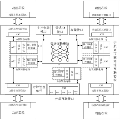
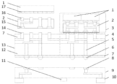
Astronavigation high-reliability high-speed interconnection core particle
PatentPendingCN117785783A
Innovation
- An aerospace high-reliability and high-speed interconnection core solution including functional core interconnection interface, external interconnection interface, protocol conversion circuit, data exchange module, clock management module, storage interface, debugging IO interface and main controller module is designed, using RS -SPC cascade code encoding and network-on-chip NoC structure realize cross-clock domain data transmission and high-reliability interconnection.
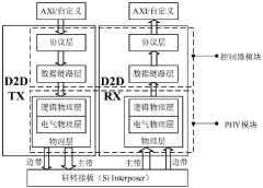
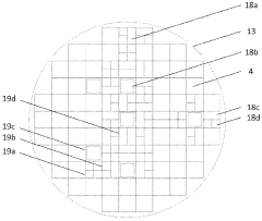
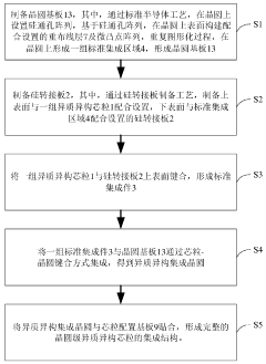
Integrated structure and integration method suitable for wafer-scale heterogeneous chiplet
PatentWO2024011880A1
Innovation
- By setting a through silicon via array and repeated standard integration areas on the wafer substrate, and preparing a silicon transfer board with heterogeneous transfer board micro-bumps and micro-pads, a standard integrated part is formed to realize heterogeneous cores. The die is bonded to the wafer substrate, and multi-layer rewiring layers are used to realize the interconnection between the die.
Aerospace Certification Standards for Semiconductor Components
Aerospace certification standards for semiconductor components represent a critical framework governing the use of advanced microelectronics in flight systems. These standards are established by regulatory bodies such as the Federal Aviation Administration (FAA), European Union Aviation Safety Agency (EASA), and the Department of Defense (DoD), each maintaining stringent requirements for components used in aerospace applications. For chiplet technology to be viable in aerospace systems, it must adhere to standards including DO-254 (Design Assurance Guidance for Airborne Electronic Hardware) and MIL-STD-883 (Test Methods for Microelectronics).
The certification process for semiconductor components in aerospace applications involves rigorous testing protocols that exceed commercial requirements. Temperature range qualification typically demands functionality from -55°C to +125°C, significantly broader than commercial (-10°C to +70°C) or even automotive (-40°C to +125°C) specifications. Radiation hardening requirements are particularly stringent, as components must withstand cosmic radiation exposure at high altitudes without experiencing single-event upsets or cumulative degradation.
Reliability standards for aerospace semiconductors mandate extensive accelerated life testing, including high-temperature operating life (HTOL) tests extending to thousands of hours. Mean Time Between Failures (MTBF) metrics for critical avionics systems often require demonstration of reliability exceeding 100,000 hours. Chiplet architectures present unique certification challenges due to their multi-die nature, requiring verification of each individual die as well as the integrated package.
Traceability requirements represent another significant aspect of aerospace certification. Each component must maintain complete manufacturing documentation, including wafer fabrication records, assembly processes, and test results. For chiplets, this becomes more complex as multiple dies from potentially different suppliers must maintain consistent documentation standards. The aerospace industry typically requires component traceability extending back 10+ years, challenging for rapidly evolving semiconductor technologies.
Quality management systems certification, particularly AS9100 (aerospace-specific extension of ISO 9001), is mandatory for suppliers providing components to aerospace manufacturers. This standard emphasizes risk management, configuration control, and prevention of counterfeit parts—all particularly relevant to chiplet integration where multiple supply chains converge in a single package. Suppliers must demonstrate robust processes for managing these risks across the entire chiplet ecosystem.
Thermal Management Strategies for Chiplets in Extreme Environments
Thermal management represents a critical challenge for chiplet integration in aerospace applications, where extreme environmental conditions demand robust solutions. Chiplets operating in aerospace environments face temperature ranges from -65°C to over 125°C, requiring thermal management strategies that ensure reliable performance across this spectrum while meeting stringent aerospace regulations.
The primary thermal management approaches for chiplets in extreme environments include advanced packaging technologies with integrated thermal interface materials (TIMs) that maintain consistent thermal conductivity across extreme temperature fluctuations. These specialized TIMs must demonstrate resilience to thermal cycling without degradation or delamination, which could compromise the thermal pathway and lead to localized hotspots.
Active cooling solutions specifically engineered for aerospace applications incorporate redundant systems to ensure continuous operation even during partial failures. These systems typically employ phase-change materials and microfluidic cooling channels that can withstand the vibration and acceleration forces encountered during launch and flight operations while maintaining compliance with aerospace weight restrictions.
Thermal simulation and modeling have become essential tools in developing chiplet thermal management strategies for extreme environments. Multi-physics simulations that account for the unique conditions of aerospace applications—including vacuum operation, radiation exposure, and rapid temperature transitions—enable engineers to identify potential thermal issues before physical prototyping begins, significantly reducing development cycles and certification timeframes.
Radiation-hardened thermal management solutions address the unique challenge of managing heat in environments with high radiation exposure. These solutions incorporate materials that maintain thermal performance despite radiation damage and include specialized heat spreading technologies that can compensate for localized heating caused by radiation events without compromising overall system reliability.
Aerospace-grade thermal monitoring systems provide real-time temperature data across chiplet arrays, enabling dynamic thermal management that can adjust cooling parameters based on operational conditions. These systems must meet DO-254 and DO-160 standards for hardware reliability and environmental testing, incorporating fail-safe mechanisms that prevent catastrophic thermal events even during system anomalies.
The integration of thermal management into the overall system architecture represents a holistic approach that considers not just the chiplets themselves but their interaction with surrounding components and the aerospace vehicle structure. This approach leverages the vehicle's thermal mass and existing cooling systems where possible, creating synergistic thermal pathways that enhance overall efficiency while meeting the strict size, weight, and power (SWaP) constraints of aerospace applications.
Unlock deeper insights with Patsnap Eureka Quick Research — get a full tech report to explore trends and direct your research. Try now!
Generate Your Research Report Instantly with AI Agent
Supercharge your innovation with Patsnap Eureka AI Agent Platform!