

How To Reduce FinFET Device Variability
SEP 11, 20259 MIN READ
Generate Your Research Report Instantly with AI Agent
PatSnap Eureka helps you evaluate technical feasibility & market potential.
FinFET Variability Background and Objectives
FinFET technology has evolved significantly since its introduction in the early 2000s as a solution to the scaling limitations of planar MOSFET devices. The three-dimensional fin structure allows for better electrostatic control of the channel, reduced short-channel effects, and improved performance at smaller technology nodes. However, as FinFET dimensions have continued to shrink below 10nm, device variability has emerged as a critical challenge affecting yield, reliability, and performance consistency in integrated circuits.
The evolution of FinFET technology has been marked by continuous efforts to enhance performance while managing increasing variability concerns. Early generations focused primarily on establishing the basic architecture and manufacturing processes, while recent developments have increasingly emphasized variability reduction techniques. Industry roadmaps indicate that managing variability will be essential for extending FinFET technology to future nodes before transitioning to alternative architectures such as Gate-All-Around (GAA) FETs.
Device variability in FinFETs manifests through several mechanisms, including random dopant fluctuations (RDF), line edge roughness (LER), fin width variations, metal gate granularity, and work function variations. These sources of variability have become more pronounced as dimensions approach atomic scales, where even minor deviations can significantly impact device characteristics. Historical data shows that threshold voltage variability (σVth) has become increasingly difficult to control below the 14nm node, with each subsequent generation requiring more sophisticated mitigation strategies.
The primary technical objective of this research is to comprehensively investigate and develop effective methods to reduce FinFET device variability while maintaining or improving performance metrics. Specifically, we aim to identify and evaluate techniques that can minimize threshold voltage variations, reduce leakage current fluctuations, and enhance overall yield in advanced FinFET processes. This includes exploring innovations in materials engineering, process optimization, device architecture modifications, and circuit-level compensation techniques.
Secondary objectives include quantifying the impact of various variability sources on device performance, establishing standardized methodologies for variability characterization, and developing predictive models that can guide future design and manufacturing decisions. Additionally, we seek to establish a comparative framework for evaluating the effectiveness and implementation feasibility of different variability reduction approaches across various application domains, from high-performance computing to ultra-low-power IoT devices.
The technological trajectory suggests that while FinFET architecture will continue to dominate in the near term, the lessons learned from addressing variability challenges will be crucial for the successful development of next-generation transistor technologies. This research aims to bridge current knowledge gaps and provide actionable insights for extending FinFET scalability through enhanced variability management.
Market Demand for Reliable FinFET Devices
The semiconductor industry's demand for reliable FinFET devices has grown exponentially as these transistors have become the backbone of modern computing systems. Market research indicates that the global FinFET technology market is projected to reach $35 billion by 2025, with a compound annual growth rate exceeding 22%. This substantial growth is primarily driven by the increasing need for high-performance, energy-efficient computing solutions across multiple sectors.
The mobile device industry represents one of the largest markets demanding reliable FinFET technology. With over 1.5 billion smartphones shipped annually, manufacturers require consistent performance and power efficiency to meet consumer expectations for longer battery life and faster processing capabilities. Device variability directly impacts yield rates, with industry reports suggesting that reducing variability by even 5% can translate to tens of millions in cost savings for high-volume production.
Data centers and cloud computing infrastructure constitute another critical market segment. As global data center traffic continues to surge, expected to reach 20.6 zettabytes annually, the need for server processors with minimal performance variation becomes paramount. Enterprise customers are willing to pay premium prices for chips that demonstrate consistent performance metrics, particularly in power consumption and computational throughput.
The automotive electronics sector presents a rapidly expanding market for FinFET technology, especially with the rise of electric vehicles and advanced driver-assistance systems. This sector demands exceptionally reliable semiconductors that can operate under varying environmental conditions with minimal performance fluctuation. Industry analysts estimate that the automotive semiconductor market will exceed $80 billion by 2026, with a significant portion requiring advanced FinFET technology.
The Internet of Things (IoT) ecosystem represents another substantial market opportunity, with billions of connected devices requiring energy-efficient, reliable microprocessors. Variability in these devices directly impacts battery life and operational consistency, which are critical factors in consumer adoption and satisfaction.
Artificial intelligence and machine learning applications have emerged as key drivers for high-performance computing needs. These workloads are particularly sensitive to computational consistency, as variability can significantly impact model training times and inference accuracy. The AI chip market is expected to grow at over 30% annually, creating strong demand for FinFETs with minimal device-to-device variation.
Market research indicates that customers across all segments are increasingly prioritizing reliability metrics in their purchasing decisions, with 78% of semiconductor buyers citing consistent performance as a "very important" factor. This trend has intensified competition among foundries to develop manufacturing processes that minimize variability, with market leaders investing billions in research and development to address this challenge.
Current Challenges in FinFET Variability Control
Despite significant advancements in FinFET technology, device variability remains a critical challenge that impacts performance, yield, and reliability in advanced semiconductor nodes. Current variability issues stem from multiple sources that become increasingly prominent as device dimensions shrink below 10nm. Random dopant fluctuation (RDF) continues to be a major contributor, where the statistical variation in dopant atom distribution significantly affects threshold voltage consistency across devices.
Line edge roughness (LER) and line width roughness (LWR) present substantial challenges during lithography and etching processes. At sub-10nm nodes, even nanometer-scale variations in fin dimensions can cause considerable performance deviations. These variations directly impact channel control and consequently affect key electrical parameters including threshold voltage, on-current, and leakage current.
Metal gate work function variability has emerged as another critical factor affecting device performance consistency. The granularity of metal gate materials and their interface with high-k dielectrics introduces variations in work function that directly translate to threshold voltage variations. This issue becomes more pronounced as gate lengths decrease, making it increasingly difficult to maintain uniform electrical characteristics.
Interface trap variations at the semiconductor-dielectric boundary further complicate variability control. These traps, which vary in density and energy distribution, cause fluctuations in carrier mobility and threshold voltage. The three-dimensional nature of FinFETs makes these interface effects more complex compared to planar devices, as multiple surfaces are involved in channel formation.
Process-induced stress variations represent another significant challenge. While stress engineering is deliberately employed to enhance carrier mobility, unintentional stress variations can lead to unpredictable device behavior. The fin formation process, including epitaxial growth and etching steps, can introduce non-uniform stress distributions that vary from device to device.
Self-heating effects have become increasingly problematic in FinFET structures due to their confined geometry and reduced thermal conductivity paths. The resulting temperature variations across the chip create additional performance inconsistencies that are difficult to model and mitigate, especially under high-performance operating conditions.
Interconnect variability further compounds these challenges, as resistance and capacitance variations in the increasingly complex back-end-of-line structures affect signal integrity and timing. The combination of front-end and back-end variability sources creates a complex multi-dimensional problem that requires holistic approaches spanning materials, process technology, device architecture, and circuit design techniques.
Existing Variability Mitigation Solutions
01 Process variations in FinFET manufacturing
Manufacturing process variations significantly impact FinFET device performance and reliability. These variations can occur in fin width, height, gate length, and oxide thickness, leading to inconsistent threshold voltages and current characteristics across devices. Advanced process control techniques and compensation methods are employed to minimize these variations and improve device uniformity in high-volume production.- Process variations in FinFET manufacturing: Manufacturing process variations significantly impact FinFET device performance and reliability. These variations include fin width fluctuations, gate length variations, and oxide thickness inconsistencies that occur during fabrication. Such variations can lead to threshold voltage shifts, leakage current increases, and overall performance degradation. Advanced process control techniques and compensation methods are employed to minimize these variations and improve device uniformity across wafers.
- Fin geometry optimization for variability reduction: The geometry of FinFET structures plays a crucial role in device variability. Optimizing fin height, width, pitch, and shape can significantly reduce performance variations. Techniques such as multi-fin designs, tapered fin profiles, and rounded fin tops help distribute electric fields more uniformly and minimize quantum effects that contribute to variability. These geometric optimizations improve threshold voltage consistency and enhance overall device reliability while maintaining performance characteristics.
- Doping strategies to control variability: Innovative doping approaches are implemented to mitigate FinFET variability issues. These include precise channel doping profiles, punch-through stoppers, and halo implants that help control short-channel effects and reduce random dopant fluctuations. Advanced techniques such as in-situ doped epitaxial growth and millisecond annealing enable more uniform dopant distribution. These strategies help maintain consistent threshold voltages across devices and improve overall circuit performance predictability.
- Modeling and simulation techniques for variability prediction: Sophisticated modeling and simulation methodologies are developed to predict and analyze FinFET device variability. These include statistical compact models, Monte Carlo simulations, and machine learning approaches that capture the impact of process variations on device performance. Advanced TCAD (Technology Computer-Aided Design) tools enable comprehensive analysis of geometric and material variations. These predictive techniques allow designers to implement variability-aware circuit design strategies and optimize manufacturing processes before fabrication.
- Circuit design techniques to mitigate FinFET variability: Circuit-level solutions are employed to address FinFET device variability challenges. These include adaptive body biasing, dynamic voltage and frequency scaling, and redundancy techniques that compensate for device-to-device variations. Self-adjusting circuits with feedback mechanisms can detect and correct for performance variations during operation. Additionally, specialized layout techniques such as common centroid arrangements and dummy structures help minimize systematic variations and improve matching between critical transistors.
02 Multi-fin designs for variability reduction
Multi-fin FinFET designs help mitigate device variability by averaging out the variations across multiple fins. By incorporating multiple fins in parallel, the overall device characteristics become more predictable and less susceptible to single-fin variations. This approach improves statistical variability and enhances performance consistency, particularly important for analog and mixed-signal applications where matching is critical.Expand Specific Solutions03 Work function engineering to control variability
Work function engineering techniques are employed to control threshold voltage variability in FinFET devices. By carefully selecting gate materials and modifying their work functions, manufacturers can achieve more consistent device performance. This approach includes using metal gates with appropriate work functions, gate stack engineering, and interface treatments to minimize random variations in threshold voltage across the chip.Expand Specific Solutions04 Doping strategies for variability management
Strategic doping approaches are implemented to manage FinFET variability. These include precise channel doping profiles, halo implants, and source/drain engineering to control short-channel effects and reduce random dopant fluctuation effects. Advanced doping techniques such as pulse doping and in-situ doped epitaxial growth help achieve more uniform electrical characteristics across devices.Expand Specific Solutions05 Simulation and modeling techniques for variability prediction
Advanced simulation and modeling techniques are developed to predict and analyze FinFET device variability. These computational methods include TCAD simulations, compact modeling, and statistical approaches that account for process variations and quantum effects. By accurately predicting variability impacts, designers can implement appropriate circuit-level compensation techniques and optimize device structures before fabrication.Expand Specific Solutions
Leading Semiconductor Companies and Research Institutions
The FinFET device variability reduction market is currently in a mature growth phase, with an estimated global market size exceeding $15 billion and expanding at 8-10% annually. Leading semiconductor manufacturers are advancing technical solutions at various maturity levels. Taiwan Semiconductor Manufacturing Co. (TSMC) and Samsung Electronics have achieved high technical maturity with production-ready variability control techniques. GlobalFoundries and IBM have developed mid-maturity solutions focusing on process optimization. SMIC and Huali are rapidly advancing their capabilities but remain at lower maturity levels. Research institutions like IMEC and Chinese Academy of Sciences' Institute of Microelectronics are pioneering next-generation approaches. The competitive landscape shows established players maintaining dominance while emerging manufacturers accelerate development to close the technology gap.
Taiwan Semiconductor Manufacturing Co., Ltd.
Technical Solution: TSMC has developed a comprehensive multi-pronged approach to reduce FinFET device variability. Their solution combines advanced process control techniques with innovative design methodologies. TSMC implements precise fin profile engineering with sub-nanometer control to ensure consistent fin dimensions across wafers. They utilize advanced lithography techniques including EUV (Extreme Ultraviolet) for critical layers to achieve better pattern fidelity and reduced line edge roughness. TSMC's proprietary strain engineering techniques optimize channel mobility while maintaining uniformity. Additionally, they employ sophisticated doping strategies with precisely controlled implant conditions and thermal budgets to minimize random dopant fluctuation effects. Their statistical process control system continuously monitors key parameters during manufacturing, enabling real-time adjustments to maintain tight process windows.
Strengths: Industry-leading EUV implementation provides superior pattern fidelity; comprehensive metrology infrastructure enables rapid feedback loops for process optimization. Weaknesses: Higher manufacturing costs associated with advanced process control systems; requires significant capital investment in cutting-edge equipment.
GlobalFoundries U.S., Inc.
Technical Solution: GlobalFoundries has developed a specialized FinFET platform with enhanced variability control features. Their approach focuses on optimizing the fin formation process through precise etch techniques and advanced sidewall smoothing methods to reduce geometric variations. They implement dual stress liner technology with carefully controlled deposition parameters to maintain consistent channel strain across the wafer. GlobalFoundries utilizes advanced statistical modeling techniques to identify and mitigate systematic variability sources during process development. Their manufacturing process incorporates feed-forward control systems that adjust subsequent process steps based on measured parameters from earlier steps, creating a self-correcting manufacturing flow. Additionally, they employ specialized annealing techniques to reduce random dopant fluctuation effects while maintaining desired dopant activation levels.
Strengths: Specialized focus on mature nodes allows for optimized variability control in specific applications; extensive experience with SOI (Silicon-On-Insulator) substrates provides additional variability reduction options. Weaknesses: Less advanced lithography capabilities compared to leading-edge manufacturers; smaller scale limits investment in some advanced process control technologies.
Key Patents and Innovations in FinFET Variability Control
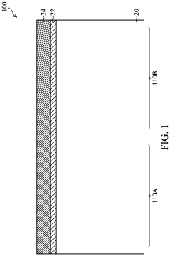
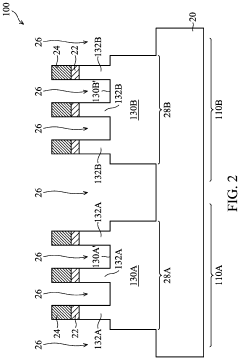
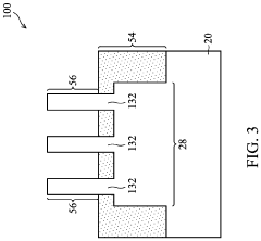
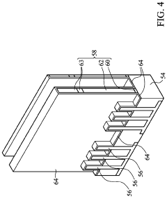
Variable size fin structures
PatentPendingUS20240363736A1
Innovation
- A method for variable fin width trimming, where fins in sparse pitch areas undergo greater width reduction than those in tight pitch areas, using silicon and silicon-germanium materials, to enhance short channel control and preserve structural integrity, involving etching and oxidation processes to define area-dependent fin widths.
FinFET Device and Method of Manufacture
PatentActiveUS20200350417A1
Innovation
- The method involves forming semiconductor fins, using a gate-last process with sacrificial layers and spacers, and a capping layer to reduce parasitic capacitive coupling, allowing for higher frequency operation and improved ring oscillator performance.
Manufacturing Process Optimization Strategies
Manufacturing process optimization represents a critical pathway to reducing FinFET device variability. The semiconductor industry has developed several sophisticated strategies to enhance manufacturing precision and consistency, directly impacting device performance uniformity.
Advanced lithography techniques form the cornerstone of variability reduction efforts. Extreme Ultraviolet (EUV) lithography, operating at 13.5nm wavelength, significantly improves pattern fidelity compared to traditional 193nm immersion lithography. This advancement enables more precise fin formation with reduced line edge roughness (LER) and line width roughness (LWR), which are primary contributors to threshold voltage variations. Implementation of multi-patterning techniques further enhances dimensional control when EUV is not available.
Process control monitoring systems have evolved to provide real-time feedback during manufacturing. Advanced metrology tools utilizing optical, electron-beam, and X-ray techniques can detect nanometer-scale variations, allowing for immediate process adjustments. Statistical Process Control (SPC) methodologies, enhanced by machine learning algorithms, can identify subtle drift patterns before they manifest as device variability issues.
Material engineering innovations have yielded significant improvements in variability reduction. Atomic Layer Deposition (ALD) enables precise layer-by-layer growth of gate dielectrics with angstrom-level thickness control. High-purity precursor materials and optimized deposition parameters minimize interface traps and fixed charges that contribute to threshold voltage variations. Similarly, advanced doping techniques like plasma doping (PLAD) and molecular monolayer doping provide more uniform dopant profiles compared to traditional ion implantation.
Thermal processing optimization plays a crucial role in managing variability. Rapid Thermal Annealing (RTA) with millisecond-level control and laser spike annealing enable precise dopant activation while minimizing diffusion. Temperature uniformity across the wafer during these processes is maintained within ±0.5°C through sophisticated heating element designs and real-time temperature mapping.
Chemical Mechanical Planarization (CMP) refinements have addressed topography-related variability issues. Dual-layer polishing pads, slurry chemistry innovations, and endpoint detection systems achieve global planarity variation below 5nm across 300mm wafers. This uniformity is essential for subsequent lithography steps and final device performance consistency.
Integration of these optimization strategies requires holistic manufacturing approaches. Design for Manufacturability (DFM) principles incorporate variability considerations from the earliest design stages. Restricted design rules limit layout configurations to those with proven manufacturing consistency, while feed-forward and feedback control loops continuously refine process parameters based on in-line measurements.
Economic Impact of FinFET Variability on Semiconductor Industry
The economic implications of FinFET device variability extend far beyond technical considerations, significantly impacting the semiconductor industry's financial landscape. Manufacturing yields, a critical economic indicator, suffer direct consequences from variability issues, with estimates suggesting that advanced FinFET processes may experience yield reductions of 15-25% due to variability-related defects. This translates to billions of dollars in lost revenue across the industry annually, particularly affecting high-volume production facilities.
Production costs escalate substantially when accounting for variability mitigation strategies. The implementation of advanced process control systems, enhanced metrology tools, and specialized design-for-manufacturing techniques adds approximately 8-12% to the overall fabrication costs. For leading-edge semiconductor manufacturers, this represents additional expenditures of $200-300 million per fabrication facility.
Time-to-market delays resulting from variability challenges create substantial opportunity costs. When chip designs require multiple iterations to address variability issues, product launches can be delayed by 3-6 months. In fast-moving semiconductor markets, such delays can reduce a product's lifetime revenue by 20-30%, particularly in consumer electronics segments where product cycles are increasingly compressed.
The economic burden of variability falls disproportionately across different industry segments. High-performance computing and server markets face the greatest financial pressure, as these applications demand the tightest performance specifications. Conversely, IoT and automotive semiconductor manufacturers often operate with wider performance margins but must meet stringent reliability requirements, creating different economic trade-offs in managing variability.
Competitive dynamics within the industry are increasingly shaped by companies' ability to manage variability effectively. Manufacturers demonstrating superior variability control command premium pricing, with evidence suggesting a 5-8% price advantage for chips with more consistent performance characteristics. This advantage compounds in high-value markets such as AI accelerators and high-performance computing, where performance predictability carries significant value.
Looking forward, economic models predict that investments in variability reduction technologies will deliver ROI ratios of 3:1 to 5:1 over five-year horizons. These projections account for both direct manufacturing improvements and the strategic market advantages of delivering more consistent products, positioning variability management as a critical economic differentiator in the semiconductor industry's future landscape.
Unlock deeper insights with PatSnap Eureka Quick Research — get a full tech report to explore trends and direct your research. Try now!
Generate Your Research Report Instantly with AI Agent
Supercharge your innovation with PatSnap Eureka AI Agent Platform!