

How To Select Atomic Force Microscopy Probes For Specific Applications
SEP 19, 20259 MIN READ
Generate Your Research Report Instantly with AI Agent
Patsnap Eureka helps you evaluate technical feasibility & market potential.
AFM Probe Technology Background and Objectives
Atomic Force Microscopy (AFM) has evolved significantly since its invention in 1986 by Gerd Binnig, Calvin Quate, and Christoph Gerber. This revolutionary scanning probe microscopy technique has transformed our ability to visualize and manipulate matter at the nanoscale, offering unprecedented resolution down to the atomic level. The technology operates by measuring forces between a sharp probe and sample surface, enabling three-dimensional surface profiling with exceptional precision.
The evolution of AFM technology has been closely tied to advancements in probe design and manufacturing. Early AFM probes were manually fabricated wires, but modern probes are sophisticated micro-engineered structures produced using semiconductor fabrication techniques. This progression has dramatically expanded the capabilities and applications of AFM across multiple scientific and industrial domains.
The primary objective of AFM probe technology is to enable precise force measurements and imaging across diverse sample types and environments. Different applications demand specific probe characteristics - from ultra-sharp tips for high-resolution imaging to specialized coatings for particular force measurements or functionalized probes for chemical and biological sensing.
Current technological trends in AFM probe development focus on several key areas: increasing durability and lifespan, enhancing resolution capabilities, developing application-specific functionalization, improving reproducibility in manufacturing, and reducing costs to broaden accessibility. These advancements aim to address existing limitations while expanding the technique's utility.
The selection of appropriate AFM probes represents a critical decision point that directly impacts measurement quality, data interpretation, and experimental success. Incorrect probe selection can lead to artifacts, data misinterpretation, sample damage, or complete measurement failure. As applications of AFM continue to diversify across fields including materials science, biology, semiconductor manufacturing, and nanotechnology, the importance of informed probe selection has grown exponentially.
This technical research aims to establish a comprehensive framework for matching AFM probe characteristics to specific application requirements. By systematically analyzing the relationship between probe properties (tip geometry, cantilever specifications, coating materials, etc.) and application demands (imaging mode, sample properties, environmental conditions, etc.), we seek to develop guidelines that optimize experimental outcomes and advance AFM capabilities across scientific and industrial applications.
The ultimate goal is to enhance measurement precision, reliability, and efficiency in AFM applications through informed probe selection strategies, thereby accelerating scientific discovery and technological innovation at the nanoscale.
Market Analysis of Application-Specific AFM Probes
The global market for Atomic Force Microscopy (AFM) probes has been experiencing steady growth, driven by increasing applications in nanotechnology, materials science, and life sciences. The market size for AFM equipment and accessories, including probes, was valued at approximately $570 million in 2022 and is projected to reach $850 million by 2028, representing a compound annual growth rate of 6.8%.
Application-specific AFM probes constitute a significant segment of this market, with specialized probes designed for particular research and industrial applications commanding premium prices due to their enhanced capabilities and performance characteristics. The materials characterization segment currently dominates the market, accounting for roughly 40% of the total demand for specialized AFM probes.
The semiconductor industry represents another major consumer of application-specific AFM probes, particularly for quality control and failure analysis processes. With the continuous miniaturization of electronic components and the development of advanced semiconductor technologies, the demand for high-precision AFM probes capable of nanoscale measurements continues to rise.
In the life sciences sector, there is growing adoption of AFM technology for biological sample imaging and biomolecular force measurements. This has created a niche market for functionalized probes designed specifically for biological applications, with an estimated market value of $75 million in 2022 and projected double-digit growth over the next five years.
Geographically, North America and Europe currently lead the market for application-specific AFM probes, collectively accounting for approximately 65% of global demand. However, the Asia-Pacific region, particularly China, Japan, and South Korea, is witnessing the fastest growth rate due to increasing investments in nanotechnology research and semiconductor manufacturing.
The competitive landscape features established players like Bruker Corporation, Oxford Instruments, and Nanosensors, who collectively hold about 70% market share. However, specialized manufacturers focusing exclusively on application-specific probes are gaining traction by offering customized solutions for niche applications.
Price sensitivity varies significantly across different market segments. Academic and research institutions tend to be more price-conscious, while industrial users in semiconductor and pharmaceutical sectors prioritize performance and reliability over cost considerations. The average selling price for standard AFM probes ranges from $30 to $100 per probe, while specialized application-specific probes can command prices between $150 and $500 depending on their unique features and capabilities.
Current Challenges in AFM Probe Selection
Despite significant advancements in atomic force microscopy (AFM) technology, probe selection remains one of the most challenging aspects for researchers and industry professionals. The primary difficulty stems from the vast array of commercially available probes with varying specifications, making it increasingly complex to identify the optimal probe for specific applications. This selection process is further complicated by the lack of standardized guidelines that comprehensively address the relationship between probe characteristics and application requirements.
A fundamental challenge is the trade-off between resolution and sample preservation. High-resolution imaging often requires sharp tips with small radii, but these probes may exert excessive pressure on delicate samples, potentially causing damage or generating artifacts. Conversely, blunter tips minimize sample damage but sacrifice resolution quality, creating a difficult balancing act for researchers working with sensitive biological specimens or nanomaterials.
Probe longevity and consistency present another significant hurdle. The mechanical wear of AFM probes during operation leads to tip degradation, altering the probe's geometry and consequently affecting measurement accuracy over time. This degradation is often unpredictable and varies based on sample hardness, scanning parameters, and environmental conditions, making it difficult to maintain consistent results throughout extended experimental sessions.
Environmental sensitivity further complicates probe selection. Factors such as humidity, temperature, and ambient electromagnetic fields can significantly impact probe performance, particularly for specialized applications like electrical or magnetic measurements. These environmental variables may necessitate specific probe coatings or designs, adding another layer of complexity to the selection process.
Cost considerations also pose substantial challenges, especially for research institutions with limited budgets. High-quality specialized probes can be prohibitively expensive, often forcing compromises between optimal performance and financial constraints. This economic factor frequently leads to suboptimal probe choices that may limit experimental outcomes or require additional validation steps.
The rapidly evolving nature of AFM applications introduces yet another challenge. As researchers push into new domains such as high-speed imaging, multiparametric measurements, and specialized force spectroscopy, the demands on probe performance become increasingly specific and stringent. Existing probe options may not fully address these emerging requirements, creating gaps between available technology and research needs.
Lastly, the interdisciplinary nature of modern AFM applications requires probe selection expertise that spans multiple scientific domains. Researchers must understand not only the mechanical properties of probes but also their chemical, electrical, and magnetic characteristics, demanding a breadth of knowledge that few individuals possess without extensive training and experience.
Application-Specific Probe Selection Methodologies
01 Probe tip design and materials
The design and material composition of AFM probe tips significantly impact measurement accuracy and resolution. Advanced tips may incorporate specialized materials like carbon nanotubes, diamond, or functionalized coatings to enhance durability, sensitivity, and chemical specificity. These designs can improve imaging resolution down to the atomic scale while reducing tip wear and sample damage during scanning operations.- Probe tip design and materials: The design and material composition of AFM probe tips significantly impact measurement accuracy and resolution. Advanced tips may incorporate specialized materials like carbon nanotubes or diamond for enhanced durability and precision. Various geometries and coatings are employed to optimize performance for specific applications, with some designs featuring multi-tip arrays for simultaneous measurements or specialized shapes for particular sample interactions.
- Cantilever design and optimization: Cantilever design is crucial for AFM probe performance, with innovations focusing on optimizing mechanical properties such as spring constant, resonance frequency, and damping characteristics. Advanced cantilevers may incorporate specialized geometries, composite materials, or integrated sensors to enhance sensitivity and reduce noise. Some designs feature temperature compensation mechanisms or specialized coatings to improve performance in various environmental conditions.
- Functionalized probes for specific applications: Functionalized AFM probes are designed for specialized applications by modifying the probe surface with specific chemical groups, biomolecules, or nanostructures. These modifications enable measurement of particular interactions such as chemical affinity, biological recognition, or electrical properties. Applications include single-molecule force spectroscopy, chemical mapping, and biological sensing, with functionalization techniques ranging from simple chemical treatments to complex biomolecular attachments.
- Probe calibration and characterization methods: Accurate calibration and characterization of AFM probes are essential for quantitative measurements. Advanced methods include in-situ calibration techniques, reference standards, and automated characterization procedures. These approaches enable precise determination of spring constants, tip geometry, and other critical parameters. Some systems incorporate real-time monitoring and feedback mechanisms to maintain calibration during measurements, enhancing measurement reliability and reproducibility.
- Multi-modal and hybrid AFM probe systems: Multi-modal and hybrid AFM probe systems combine traditional AFM capabilities with other measurement techniques in a single probe. These integrated systems may incorporate electrical, thermal, optical, or magnetic sensing capabilities alongside topographical measurements. Advanced designs feature specialized probe architectures that enable simultaneous acquisition of multiple data types, providing comprehensive sample characterization. Applications include nanoscale electrical characterization, thermal analysis, and optical-mechanical property mapping.
02 Cantilever optimization and fabrication
Cantilever design is crucial for AFM probe performance, with innovations focusing on optimizing spring constants, resonance frequencies, and damping characteristics. Advanced fabrication techniques enable the production of cantilevers with precise dimensions and mechanical properties. These optimizations improve force sensitivity, reduce noise, and enhance measurement stability across various operating environments and sample types.Expand Specific Solutions03 Multi-functional and specialized probes
Specialized AFM probes are designed for specific applications such as electrical measurements, magnetic force microscopy, or biological sample imaging. These probes may incorporate additional sensing elements, electrodes, or functional coatings to enable simultaneous measurement of multiple sample properties. Such multi-functional capabilities expand the analytical power of AFM beyond topographical imaging to include electrical, magnetic, thermal, and chemical characterization.Expand Specific Solutions04 Calibration and measurement accuracy
Accurate calibration of AFM probes is essential for quantitative measurements. Innovations in this area include automated calibration methods, reference standards, and algorithms for determining probe parameters such as spring constants and tip geometry. These advances improve measurement reproducibility and enable more accurate force measurements, dimensional analysis, and material property characterization across different samples and operating conditions.Expand Specific Solutions05 Environmental and operational adaptations
AFM probes designed for specific environmental conditions enable measurements in liquid media, vacuum, variable temperatures, or other challenging environments. These specialized probes may feature protective coatings, temperature compensation mechanisms, or designs that minimize drift and interference. Such adaptations extend the application range of AFM to in-situ studies of dynamic processes, biological samples in physiological conditions, and materials under various environmental stresses.Expand Specific Solutions
Leading Manufacturers and Research Institutions
The atomic force microscopy (AFM) probe selection market is currently in a growth phase, characterized by increasing specialization for diverse applications. The global AFM market is estimated at approximately $500 million, with probes representing a significant segment experiencing steady annual growth of 5-8%. Technologically, the field shows varying maturity levels across applications, with established players like Bruker Nano, Oxford Instruments Asylum Research, and Keysight Technologies leading commercial innovation. Research institutions including Georgia Tech Research Corp, CNRS, and various universities are advancing fundamental probe technologies. Emerging players such as Infinitesima are introducing disruptive technologies like Rapid Probe Microscopy, while established corporations including Agilent, Texas Instruments, and Western Digital are developing application-specific solutions for semiconductor, materials science, and data storage industries.
Bruker Nano, Inc.
Technical Solution: Bruker Nano has developed a comprehensive suite of atomic force microscopy (AFM) probes tailored for specific applications. Their SCANASYST-AIR probes utilize Peak Force Tapping technology, which automatically optimizes imaging parameters while providing force control to prevent sample damage. For biological applications, they offer the DNP series with silicon nitride cantilevers featuring multiple probe options on a single chip, allowing researchers to select the optimal spring constant for their specific biomolecule or cell type. Their RTESPA-300 probes incorporate antimony-doped silicon for electrical measurements with wear-resistant tips. Bruker's FastScan probes are designed with small cantilevers that enable high-speed imaging up to 10x faster than conventional probes while maintaining resolution. Their specialized PFQNM-LC probes feature pre-calibrated spring constants for quantitative nanomechanical mapping, eliminating the need for time-consuming calibration procedures.
Strengths: Bruker's probes offer application-specific designs with pre-calibrated options that reduce setup time and improve measurement accuracy. Their Peak Force Tapping technology provides superior force control, preventing sample damage. Weaknesses: Their specialized probes tend to be more expensive than generic alternatives, and some of their advanced features require proprietary Bruker AFM systems to fully utilize all capabilities.
Agilent Technologies, Inc.
Technical Solution: Agilent Technologies has developed a systematic approach to AFM probe selection through their PicoView software platform, which guides users through probe selection based on application requirements. Their MAC Mode III technology utilizes magnetic actuation of probes for enhanced performance in liquid environments, particularly valuable for biological samples. Agilent's SSS-NCHR SuperSharp Silicon probes feature tip radii of less than 2nm, enabling ultra-high resolution imaging of nanoscale features. For specialized applications, they've developed the ACCESS-NC probes with offset tips that allow imaging of deep trenches and high-aspect-ratio structures commonly found in semiconductor applications. Their temperature-resistant OMCL-AC160TS probes maintain performance stability across a wide temperature range (up to 200°C), making them suitable for thermal analysis applications. Agilent's probe selection methodology incorporates an application-specific decision tree that considers sample characteristics, environmental conditions, and measurement objectives.
Strengths: Agilent's probes excel in specialized environments, particularly liquid imaging for biological samples, with their magnetic actuation technology reducing noise and improving stability. Their software-guided selection process simplifies probe choice for new users. Weaknesses: Their probe lineup has fewer options for some specialized applications compared to market leaders, and integration with non-Agilent systems may require additional adapters or modifications.
Critical Parameters for Optimizing Probe Performance
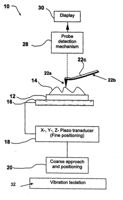
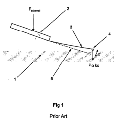
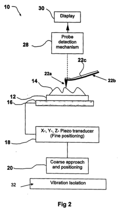
Probe for an atomic force microscope
PatentInactiveUS20070024295A1
Innovation
- A probe with a force sensing member and a tip radius of 100 nm or less, adapted to experience a biasing force greater than the restoring force during scanning, allowing for improved tracking and faster scanning speeds by incorporating a biasing element responsive to external forces or a low Q factor cantilever beam to dissipate mechanical energy.
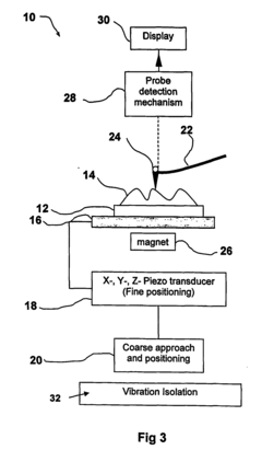
Atomic force microscopy probe
PatentActiveUS8091143B2
Innovation
- The use of a micromechanical resonator oscillating in a volume mode, with a tip projecting from an antinode point, allows for selective excitation and detection of oscillations, enhancing sensitivity and time resolution, and is fabricated using conventional lithographic techniques.

Material Compatibility Considerations
Material compatibility is a critical factor when selecting atomic force microscopy (AFM) probes for specific applications. Different sample materials interact uniquely with probe materials, affecting measurement accuracy, probe longevity, and data quality. Understanding these interactions is essential for optimizing experimental outcomes.
The hardness differential between probe and sample materials significantly impacts measurement results. When probing soft materials like polymers or biological samples, silicon or silicon nitride probes with lower spring constants are typically preferred to prevent sample deformation. Conversely, harder materials such as ceramics or metals may require diamond-coated or solid diamond probes to minimize tip wear and maintain measurement consistency throughout extended scanning sessions.
Chemical compatibility must also be considered, particularly when working in liquid environments or with reactive samples. Silicon probes can be unsuitable for studies in strong acidic or basic solutions due to potential chemical degradation. In such cases, gold-coated or platinum-iridium probes offer superior chemical resistance. For biological applications, functionalized probes with specific chemical groups may be necessary to achieve desired interactions with biomolecules.
Electrical and magnetic properties of both probe and sample materials create another dimension of compatibility considerations. Conductive samples require conductive probes (typically metal-coated) for techniques like conductive AFM or Kelvin probe force microscopy. Similarly, magnetic force microscopy necessitates probes with magnetic coatings that are compatible with the magnetic domains being studied without causing excessive interference.
Temperature compatibility becomes crucial for thermal applications or environmental studies. Standard silicon probes may experience significant property changes at elevated temperatures, whereas specialized high-temperature probes maintain their mechanical properties across wider temperature ranges. The thermal expansion coefficient difference between probe and sample materials can introduce measurement artifacts if not properly accounted for.
Surface energy compatibility affects tip-sample adhesion forces, which can dominate interactions in certain applications. Hydrophilic samples may require hydrophilic probes to maintain consistent contact, while hydrophobic coatings might be beneficial when working with water-repellent surfaces. This consideration is particularly important in force spectroscopy applications where adhesion forces are directly measured.
Finally, contamination potential between probe and sample materials must be evaluated, especially for ultra-clean applications or when working with sensitive samples. Some coating materials may shed particles or leach chemicals that could contaminate samples, compromising experimental integrity. Selecting inert materials or appropriate pre-treatment protocols can mitigate these risks.
Cost-Benefit Analysis of Specialized Probes
When evaluating the cost-benefit ratio of specialized Atomic Force Microscopy (AFM) probes, organizations must consider both immediate expenditures and long-term value. Standard silicon or silicon nitride probes typically range from $20-50 per unit, while specialized probes with custom coatings or functionalization can cost $100-500 or more. This significant price differential necessitates careful analysis of application requirements and expected outcomes.
High-resolution imaging applications may justify premium probes with ultra-sharp tips, as the enhanced data quality can reduce the need for repeated measurements and accelerate research timelines. For instance, in semiconductor quality control, investing in specialized conductive probes at $200-300 per unit can yield substantial returns by identifying nanoscale defects that might otherwise cause device failures worth thousands of dollars.
The durability factor presents another important consideration. While standard probes may require replacement after 10-20 scans, specialized probes with diamond-like carbon coatings can withstand hundreds of measurements, potentially offering better long-term value despite higher initial costs. This becomes particularly relevant in industrial applications where continuous monitoring is required.
Research institutions should evaluate specialized probes against their specific scientific objectives. A university laboratory conducting fundamental research might benefit more from purchasing various probe types to explore different sample properties, whereas industrial R&D departments might prioritize consistency and reproducibility offered by premium probes for specific applications.
The learning curve associated with specialized probes represents a hidden cost. Staff training and optimization time must be factored into the total investment. However, once mastered, specialized probes often enable more efficient workflows and reduce sample preparation requirements, creating operational savings that offset initial expenditures.
Maintenance costs vary significantly between probe types. Some specialized probes require careful storage conditions or cleaning protocols that add to their total cost of ownership. Conversely, certain premium probes with protective coatings may reduce maintenance requirements, providing value through extended usability.
Organizations should implement a systematic evaluation framework that considers application criticality, measurement frequency, required resolution, and budget constraints. For high-volume routine measurements, the economics might favor standard probes, while precision-critical applications often demonstrate positive returns on investment for specialized options despite their premium pricing.
Unlock deeper insights with Patsnap Eureka Quick Research — get a full tech report to explore trends and direct your research. Try now!
Generate Your Research Report Instantly with AI Agent
Supercharge your innovation with Patsnap Eureka AI Agent Platform!