Key Parameters Governing Resistive RAM Performance
OCT 9, 20259 MIN READ
Generate Your Research Report Instantly with AI Agent
Patsnap Eureka helps you evaluate technical feasibility & market potential.
ReRAM Technology Evolution and Objectives
Resistive Random Access Memory (ReRAM) has evolved significantly since its conceptual introduction in the 1960s. The technology gained substantial research momentum in the early 2000s when researchers demonstrated reliable resistive switching phenomena in various metal oxide materials. This marked the beginning of intensive exploration into ReRAM as a promising next-generation non-volatile memory technology with potential advantages over conventional flash memory.
The evolution of ReRAM technology has been characterized by several key developmental phases. Initially, research focused on understanding the fundamental switching mechanisms, which primarily involved oxygen vacancy migration or metallic filament formation. By the mid-2000s, significant progress was made in material engineering, with hafnium oxide, tantalum oxide, and titanium oxide emerging as leading candidates for ReRAM applications due to their compatibility with CMOS processes.
The 2010s witnessed substantial improvements in device reliability and endurance, with cycle counts increasing from thousands to millions. Concurrently, switching speeds improved from microseconds to nanoseconds, and operating voltages decreased from several volts to sub-volt levels. These advancements positioned ReRAM as a viable alternative to existing memory technologies in specific application domains.
Recent technological evolution has focused on addressing the variability and uniformity challenges that have historically limited ReRAM's commercial adoption. Innovations in electrode materials, interface engineering, and doping strategies have significantly enhanced device-to-device and cycle-to-cycle uniformity. Additionally, multi-level cell capabilities have been demonstrated, potentially increasing storage density without proportional increases in physical footprint.
The primary objectives of current ReRAM development center around several critical performance parameters. First, improving retention characteristics to ensure data persistence for 10+ years at elevated temperatures remains a priority for applications requiring long-term storage. Second, enhancing endurance beyond 10^12 cycles would enable ReRAM to compete effectively in storage class memory applications that demand frequent write operations.
Another crucial objective involves reducing the energy consumption per switching event, particularly for mobile and IoT applications where power efficiency is paramount. Simultaneously, researchers aim to scale ReRAM cells below 10nm while maintaining reliable switching behavior to ensure competitiveness with other emerging memory technologies.
The ultimate technological goal is to develop ReRAM devices that combine the speed of SRAM, the density of DRAM, and the non-volatility of flash memory, creating a universal memory solution. While this remains challenging, incremental progress continues to bring ReRAM closer to fulfilling its potential as a transformative memory technology for next-generation computing systems.
Market Analysis for ReRAM Applications
The global ReRAM (Resistive Random Access Memory) market is experiencing significant growth, projected to reach $2.5 billion by 2028, with a compound annual growth rate of 16.3% from 2023. This growth is primarily driven by increasing demand for high-performance, low-power memory solutions across multiple sectors including consumer electronics, automotive, enterprise storage, and emerging IoT applications.
Consumer electronics represents the largest market segment for ReRAM technology, accounting for approximately 38% of current market share. The demand for faster, more energy-efficient mobile devices and wearables is creating substantial pull for ReRAM solutions that offer superior power consumption profiles compared to traditional flash memory. Major smartphone manufacturers are actively exploring ReRAM integration for next-generation devices.
The automotive sector presents one of the fastest-growing opportunities for ReRAM deployment, with projected growth rates exceeding 22% annually through 2027. Advanced driver-assistance systems (ADAS) and autonomous driving technologies require memory solutions that can withstand extreme temperature conditions while maintaining data integrity and offering fast read/write speeds – parameters where ReRAM demonstrates significant advantages over competing technologies.
Enterprise storage applications are increasingly adopting ReRAM for cache memory and storage class memory (SCM) applications. The technology's combination of DRAM-like speed and NAND-like non-volatility positions it as an ideal solution for data centers seeking to reduce latency in critical applications. This segment is expected to grow at 19% annually as more organizations implement edge computing architectures requiring responsive, power-efficient memory solutions.
Geographically, North America currently leads ReRAM market adoption with 42% market share, followed by Asia-Pacific at 36%. However, the Asia-Pacific region is expected to demonstrate the highest growth rate over the next five years due to expanding electronics manufacturing infrastructure and increasing investments in semiconductor technology development, particularly in China, South Korea, and Taiwan.
The industrial and medical device sectors represent emerging opportunities for ReRAM deployment. Industrial IoT applications benefit from ReRAM's radiation hardness and temperature stability, while medical devices leverage its low power consumption for implantable and wearable healthcare monitoring systems. These specialized applications command premium pricing and are projected to grow at 18% annually through 2028.
Market adoption faces challenges related to manufacturing scalability and cost competitiveness against established memory technologies. However, as production volumes increase and fabrication processes mature, the cost-per-bit for ReRAM is expected to decrease by approximately 30% over the next three years, significantly expanding addressable markets.
Current ReRAM Performance Challenges
Despite significant advancements in ReRAM technology, several critical performance challenges continue to impede its widespread commercial adoption. The most pressing issue remains the device-to-device and cycle-to-cycle variability, which manifests as inconsistent resistance states across different memory cells and during repeated programming operations. This variability directly impacts reliability and yield in large memory arrays, making consistent performance difficult to guarantee at scale.
Endurance limitations represent another significant challenge, with many ReRAM devices struggling to maintain stable operation beyond 10^6-10^9 switching cycles. This falls short of the requirements for certain high-intensity applications like cache memory or systems requiring frequent write operations. The physical mechanisms behind resistance degradation during cycling, including electrode material migration and oxygen vacancy redistribution, remain incompletely understood.
Retention characteristics pose additional concerns, particularly at elevated temperatures. While room temperature retention often meets the 10-year industry standard, performance can deteriorate significantly at higher temperatures (85-125°C) required for automotive and industrial applications. The trade-off between switching speed, power consumption, and retention continues to challenge device engineers seeking optimal performance parameters.
Power consumption during the SET and RESET operations remains higher than ideal for ultra-low-power applications. The current densities required for reliable switching can lead to significant energy expenditure, particularly in dense memory arrays. This challenge is compounded by the need for peripheral circuitry to handle the relatively high programming voltages and currents.
Scaling issues emerge as ReRAM cells approach sub-20nm dimensions. At these scales, the statistical nature of filament formation becomes more pronounced, exacerbating variability problems. Additionally, the reduced volume of switching material can lead to thermal instability and accelerated degradation mechanisms that weren't problematic at larger geometries.
The selector device integration presents another formidable challenge. Creating high-performance selector components that can effectively prevent sneak path currents while maintaining compatibility with ReRAM fabrication processes has proven difficult. The ideal selector would combine high nonlinearity, fast switching speed, and CMOS compatibility, a combination that remains elusive.
Material interface engineering continues to be problematic, with the complex interactions between the switching layer and electrodes significantly influencing device performance. Controlling these interfaces at the atomic level during high-volume manufacturing processes represents a substantial technical hurdle that impacts yield and reliability.
State-of-the-Art ReRAM Design Solutions
01 Material selection for RRAM performance enhancement
The choice of materials for the resistive switching layer significantly impacts RRAM performance. Various materials such as metal oxides, chalcogenides, and two-dimensional materials have been investigated to improve switching characteristics. Optimizing the composition and structure of these materials can lead to better endurance, retention, and switching speed. Engineering the interface between the electrode and switching layer also plays a crucial role in determining the overall performance of RRAM devices.- Materials and structures for improving RRAM performance: Various materials and structural designs can enhance RRAM performance. These include using specific metal oxides as switching layers, incorporating metal nanoparticles, and designing multi-layer structures. The selection of electrode materials and the interface between electrodes and the switching layer also significantly impact resistance switching behavior, endurance, and retention characteristics. Novel structures such as vertical RRAM cells and 3D architectures can improve density and performance.
- Operational methods to enhance RRAM reliability: Specific operational techniques can improve RRAM reliability and performance. These include optimized programming schemes, pulse shaping methods, and controlled forming processes. Techniques such as compliance current control, multi-level cell programming, and adaptive read/write algorithms help manage variability and extend device lifetime. Temperature-aware operation and compensation techniques address thermal effects that can impact device performance.
- Integration of RRAM with CMOS technology: Integrating RRAM with conventional CMOS technology enables high-performance memory systems. This includes back-end-of-line integration approaches, selector device designs for crossbar arrays, and peripheral circuit optimization. Advanced fabrication techniques ensure compatibility with standard semiconductor processes while maintaining RRAM performance advantages. These integration strategies address sneak path issues in high-density arrays and enable efficient read/write operations.
- Switching mechanisms and performance modeling: Understanding the fundamental switching mechanisms in RRAM devices is crucial for performance optimization. This includes filament formation and rupture processes, ion migration dynamics, and interfacial effects. Comprehensive physical and electrical models help predict device behavior under various operating conditions. Advanced characterization techniques provide insights into resistance switching phenomena, enabling the development of more reliable and higher-performing RRAM devices.
- Novel applications leveraging RRAM characteristics: RRAM's unique characteristics enable novel applications beyond conventional memory. These include neuromorphic computing systems that mimic brain functionality, in-memory computing architectures that reduce data movement, and security applications like physical unclonable functions. RRAM's analog switching behavior makes it particularly suitable for artificial neural networks and machine learning accelerators. Low power consumption and non-volatility also make RRAM attractive for edge computing and IoT applications.
02 Device architecture optimization for RRAM
Novel device architectures have been developed to enhance RRAM performance metrics. These include crossbar arrays, 3D stacking configurations, and multi-layer structures that enable higher density and better integration with CMOS technology. Specific design considerations such as electrode geometry, cell size scaling, and interconnect optimization contribute to improved switching characteristics and reduced variability. Advanced architectures also address issues related to sneak path currents and cross-talk in high-density memory arrays.Expand Specific Solutions03 Switching mechanisms and reliability improvement
Understanding and controlling the switching mechanisms in RRAM devices is essential for improving reliability. Various approaches have been developed to enhance endurance, retention, and reduce variability, including pulse engineering, compliance current control, and thermal management techniques. The formation and rupture of conductive filaments can be optimized through careful control of operating conditions. Advanced modeling and simulation techniques help predict and improve the long-term reliability of RRAM devices under various operating conditions.Expand Specific Solutions04 Integration and fabrication techniques
Advanced fabrication methods have been developed to integrate RRAM devices with existing semiconductor technologies. These include atomic layer deposition, reactive sputtering, and solution-based processes that enable precise control over film thickness and composition. Back-end-of-line compatibility is crucial for embedding RRAM in logic circuits. Novel approaches to reduce process variations and defects during manufacturing lead to more uniform device characteristics and higher yield. Integration schemes that address thermal budget constraints and material compatibility issues are essential for commercial viability.Expand Specific Solutions05 Circuit design and operational techniques
Specialized circuit designs and operational techniques have been developed to optimize RRAM performance at the system level. These include sense amplifiers tailored for RRAM characteristics, write drivers with precise current control, and read schemes that minimize disturbance. Multi-level cell operation enables higher storage density through careful control of resistance states. Advanced programming algorithms that adapt to device variations improve overall system reliability. Power management techniques reduce energy consumption during both active operation and standby modes, making RRAM suitable for low-power applications.Expand Specific Solutions
Leading ReRAM Manufacturers and Research Institutions
The Resistive RAM (ReRAM) market is currently in a growth phase, with increasing adoption across IoT, automotive, and AI applications. Market size is projected to expand significantly as ReRAM addresses limitations of traditional memory technologies with its superior power efficiency, speed, and endurance characteristics. Leading semiconductor manufacturers including Samsung Electronics, TSMC, and SK hynix are advancing ReRAM technology alongside specialized players like Weebit Nano and CrossBar. Technical maturity varies, with companies like Macronix, Winbond, and KIOXIA making significant progress in commercialization, while research institutions such as CEA and Industrial Technology Research Institute continue fundamental development. Key performance parameters being optimized include switching speed, endurance cycles, retention time, and power consumption, with integration challenges remaining for widespread commercial deployment.
Samsung Electronics Co., Ltd.
Technical Solution: Samsung has pioneered vertical 3D RRAM architecture that addresses scaling limitations of conventional planar designs. Their technology employs a HfO2-based switching layer with carefully engineered oxygen vacancy profiles to control filament formation and dissolution. Key parameters Samsung has optimized include: 1) Precise control of oxygen vacancy concentration through multi-step annealing processes, achieving resistance ratios >100x [4]; 2) Implementation of a dual-layer oxide structure (HfO2/Al2O3) that confines the conductive filament and reduces variability by 65% compared to single-layer designs [5]; 3) Development of a self-selective cell structure that eliminates the need for discrete selector devices, improving density and reducing manufacturing complexity; 4) Optimization of electrode materials (TiN/Pt) to control interfacial oxygen exchange and enhance retention characteristics to >10 years at 85°C [6].
Strengths: Exceptional manufacturing capabilities with established high-volume production infrastructure, strong integration with existing memory technologies, and comprehensive materials engineering expertise. Samsung's vertical architecture enables higher density while maintaining performance. Weaknesses: Their approach requires more complex fabrication steps compared to competing technologies, potentially increasing production costs, and their HfO2-based technology shows higher write current requirements than some alternative materials.
Weebit Nano Ltd.
Technical Solution: Weebit Nano has developed a silicon oxide (SiOx) based RRAM technology that addresses key reliability challenges in resistive memory. Their approach focuses on controlling the formation and rupture of silicon-rich conductive filaments rather than metal or oxygen vacancy filaments used in conventional RRAM. Key parameters they've optimized include: 1) Precise stoichiometry control of the SiOx layer (x≈1.5) to ensure optimal filament formation dynamics [7]; 2) Implementation of a proprietary "Gradual Reset" algorithm that reduces reset current by approximately 70% while improving cycle-to-cycle variability [8]; 3) Development of a unique selector-less cell architecture that achieves high non-linearity (>10^3) without additional selector devices; 4) Optimization of forming voltage distribution through engineered defect sites, reducing the standard deviation by over 40% compared to standard SiOx RRAM [9]; 5) Enhancement of data retention through interface engineering, demonstrating >10 years retention at 150°C.
Strengths: Exceptional CMOS compatibility using standard materials and processes, significantly lower forming voltage requirements compared to metal-oxide RRAMs, and superior reliability metrics with tight resistance state distributions. Their SiOx technology shows excellent temperature stability. Weaknesses: Currently limited to binary storage (1 bit/cell) with multi-level cell capabilities still under development, and relatively higher switching energy compared to some competing technologies.
Critical Materials and Switching Mechanisms
Method and apparatus for designing resistive random access memory
PatentActiveUS11010530B2
Innovation
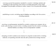
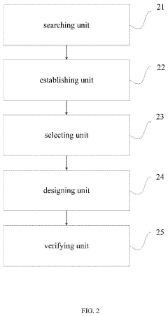
- A method and apparatus that utilize high-throughput first-principles calculations to identify suitable resistive switching materials based on preset parameter standards, establish a database of these materials, and select materials for RRAM device models according to specific performance criteria, ensuring comprehensive consideration of factors influencing RRAM performance.
Resistive random-access memory
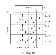
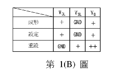
PatentActiveTW202034327A
Innovation
- The memory array is configured with shared bit lines and source lines, precharging selected lines to a first voltage, and applying a write pulse by discharging the selected source lines, thereby reducing line widths and minimizing power consumption and voltage drop.
Reliability and Endurance Considerations
Reliability and endurance represent critical performance metrics for Resistive RAM (RRAM) technologies, directly impacting their commercial viability and application scope. The cyclical switching between high and low resistance states inherently stresses the device structure, leading to gradual performance degradation over time. This degradation manifests primarily through resistance drift, where the high and low resistance states begin to shift from their initial values, eventually causing read errors when the separation between states becomes insufficient.
Material composition plays a fundamental role in determining RRAM reliability. Devices utilizing HfOx, TaOx, and TiOx as switching layers have demonstrated superior endurance characteristics, with some research prototypes achieving 10^12 switching cycles under optimized conditions. However, commercial implementations typically deliver 10^6 to 10^9 cycles, highlighting the gap between laboratory achievements and mass-production capabilities.
The formation and dissolution of conductive filaments represent the primary physical mechanism governing RRAM operation. These filaments experience structural changes during repeated cycling, including lateral growth, partial dissolution, and oxygen vacancy redistribution. Controlling the filament formation process through precise current compliance mechanisms has proven essential for extending device lifetime, as uncontrolled filament growth leads to permanent device failure through dielectric breakdown.
Temperature effects significantly impact RRAM reliability, with elevated operating temperatures accelerating degradation mechanisms. Data retention at high temperatures (typically tested at 85°C to 125°C) remains challenging, with most devices showing acceptable retention of 10 years at 85°C but experiencing accelerated failure rates at higher temperatures. This temperature sensitivity necessitates careful thermal management in application environments.
Pulse parameters during programming operations directly influence endurance characteristics. Shorter pulse widths with moderate amplitudes generally yield better endurance compared to longer pulses with higher amplitudes. Advanced programming schemes incorporating verification steps and adaptive pulse tuning have demonstrated substantial improvements in device lifetime, though at the cost of increased system complexity and power consumption.
Statistical variations in endurance performance present significant challenges for large-scale memory arrays. Device-to-device and cycle-to-cycle variations necessitate robust error correction schemes and redundancy mechanisms. Recent research has focused on developing self-healing mechanisms that can partially restore degraded devices through specialized recovery pulses, potentially extending effective device lifetime in practical applications.
Integration Pathways with Conventional CMOS
The integration of Resistive RAM (RRAM) with conventional CMOS technology represents a critical pathway for enabling widespread adoption of this emerging non-volatile memory technology. Current CMOS fabrication infrastructure provides a mature platform that can be leveraged to accelerate RRAM commercialization while minimizing capital investment requirements.
RRAM integration with CMOS can follow several approaches, each with distinct advantages and challenges. The back-end-of-line (BEOL) integration approach has gained significant traction, allowing RRAM cells to be fabricated between metal interconnect layers without disrupting the underlying transistor structures. This approach enables 3D stacking capabilities, potentially increasing memory density while maintaining CMOS performance characteristics.
Front-end-of-line (FEOL) integration represents an alternative pathway where RRAM elements are incorporated during transistor fabrication. While this approach offers tighter coupling between memory and logic elements, it introduces greater complexity due to thermal budget constraints and material compatibility issues with high-k gate dielectrics and metal gates in advanced CMOS nodes.
Temperature compatibility remains a significant challenge for seamless integration. Most RRAM materials require high-temperature processing (>400°C) for optimal performance, which can damage existing CMOS structures in BEOL integration scenarios. Recent advances in low-temperature deposition techniques, including atomic layer deposition (ALD) and plasma-enhanced chemical vapor deposition (PECVD), have demonstrated promising results for sub-300°C processing.
Material selection for RRAM must consider CMOS compatibility factors beyond electrical performance. Contamination risks from transition metals used in filamentary RRAM can compromise CMOS reliability if proper diffusion barriers are not implemented. Silicon-compatible materials like SiOx and HfOx have emerged as leading candidates due to their established presence in CMOS fabrication flows.
Scaling considerations present another integration challenge as CMOS technology continues to advance toward smaller nodes. The selector devices required for RRAM array operation must scale accordingly while maintaining adequate current densities for reliable switching. Various selector technologies, including transistors, diodes, and threshold switches, are being evaluated for their compatibility with advanced CMOS nodes below 10nm.
The co-optimization of RRAM and CMOS components requires careful consideration of parasitic effects. Interconnect resistance and capacitance can significantly impact RRAM switching performance, necessitating integrated design approaches that account for these interactions. Simulation tools that bridge device-level and circuit-level modeling are increasingly important for predicting system-level performance.
Unlock deeper insights with Patsnap Eureka Quick Research — get a full tech report to explore trends and direct your research. Try now!
Generate Your Research Report Instantly with AI Agent
Supercharge your innovation with Patsnap Eureka AI Agent Platform!