

OLED vs MicroLED: Semiconductor Channel Structure Evolution
OCT 24, 20259 MIN READ
Generate Your Research Report Instantly with AI Agent
PatSnap Eureka helps you evaluate technical feasibility & market potential.
Display Technology Evolution and Objectives
Display technology has undergone remarkable evolution since the introduction of cathode ray tubes (CRTs) in the early 20th century. The progression from CRTs to liquid crystal displays (LCDs) marked the first major shift in display technology, enabling thinner, more energy-efficient screens. The subsequent development of organic light-emitting diode (OLED) technology in the late 1980s represented another significant advancement, offering superior contrast ratios, wider viewing angles, and the ability to create flexible displays.
OLED technology utilizes organic compounds that emit light when an electric current is applied. The semiconductor channel structure in OLEDs consists of multiple organic layers sandwiched between two electrodes. This structure allows for self-emissive pixels that don't require backlighting, resulting in deeper blacks and more vibrant colors compared to LCD technology. However, OLEDs face challenges related to limited lifespan, particularly for blue emitters, and susceptibility to burn-in effects.
MicroLED technology emerged as a promising alternative in the early 2000s, addressing many of OLED's limitations. MicroLEDs employ inorganic semiconductor materials, typically gallium nitride (GaN), to create arrays of microscopic LED structures. The semiconductor channel structure in MicroLEDs features a more robust inorganic composition, offering significantly improved brightness, efficiency, and longevity compared to OLEDs.
The evolution of semiconductor channel structures in display technologies reflects a continuous pursuit of enhanced performance metrics: higher resolution, improved energy efficiency, better color accuracy, and increased durability. The transition from organic to inorganic semiconductor materials represents a fundamental shift in approach, with each technology offering distinct advantages and limitations.
Current technological objectives in the display industry focus on several key areas: achieving higher pixel densities for applications in virtual and augmented reality; developing more energy-efficient displays for mobile devices; improving manufacturing processes to reduce costs; and enhancing durability and lifespan, particularly for flexible and foldable displays.
The semiconductor channel structure evolution from OLED to MicroLED also aims to address specific technical challenges, including reducing pixel size while maintaining brightness, improving quantum efficiency, minimizing power consumption, and enhancing color gamut coverage. These objectives drive ongoing research into novel semiconductor materials and innovative channel structures.
Looking forward, the industry is exploring hybrid approaches that combine the strengths of both OLED and MicroLED technologies, as well as investigating entirely new display paradigms such as quantum dot displays and holographic technologies. The ultimate goal remains creating display technologies that deliver immersive, lifelike visual experiences while minimizing energy consumption and maximizing device longevity.
Market Demand Analysis for Advanced Display Technologies
The display technology market is witnessing unprecedented growth driven by increasing consumer demand for superior visual experiences across multiple device categories. Current market analysis indicates that the global advanced display market is projected to reach $167 billion by 2025, with OLED technology currently dominating premium segments while MicroLED emerges as a promising challenger. This growth trajectory is supported by expanding applications in smartphones, televisions, wearables, automotive displays, and commercial signage.
Consumer preferences are increasingly favoring thinner, more energy-efficient displays with higher resolution, better color accuracy, and longer lifespans. OLED technology has established market dominance due to its superior contrast ratios, flexibility, and power efficiency in dark scenes. However, research indicates growing consumer awareness and interest in MicroLED's potential advantages, particularly regarding brightness capabilities and longevity.
The smartphone segment represents the largest market share for advanced display technologies, with premium manufacturers transitioning toward OLED as standard. Apple's adoption of OLED across its iPhone lineup has significantly influenced market direction. Meanwhile, the television sector is experiencing rapid transformation with Samsung, LG, and Sony competing to commercialize next-generation display technologies at increasingly accessible price points.
Emerging applications in automotive displays present substantial growth opportunities, with projections indicating a 24% CAGR through 2027. Advanced driver information systems and passenger entertainment displays are driving demand for both OLED and potential MicroLED implementations. Additionally, the wearable technology segment requires displays with exceptional power efficiency and durability characteristics that both technologies can potentially address.
Regional analysis reveals Asia-Pacific as the dominant manufacturing hub, while North America and Europe lead in technology innovation and premium market adoption. China's aggressive investment in display manufacturing infrastructure is reshaping global supply chains and accelerating commercialization timelines for both technologies.
Industry surveys indicate that manufacturers are increasingly focused on semiconductor channel structure evolution as a critical differentiator. The transition from traditional OLED structures to more advanced architectures, alongside MicroLED's fundamentally different approach to pixel formation, represents a pivotal competitive battleground. Market research suggests that companies capable of achieving breakthroughs in semiconductor channel efficiency, particularly in electron mobility and stability, will secure significant competitive advantages in the next generation of display products.
OLED and MicroLED Technical Challenges
Both OLED and MicroLED technologies face significant technical challenges that impact their commercial viability and performance capabilities. OLED technology, despite its market maturity, continues to struggle with several fundamental issues. Lifetime degradation remains a critical concern, particularly for blue OLED emitters which typically degrade faster than red and green counterparts, creating color balance issues over time. This differential aging necessitates complex compensation algorithms and hardware solutions that increase manufacturing complexity.
Material stability presents another major challenge for OLED displays. The organic materials are susceptible to moisture and oxygen, requiring sophisticated encapsulation techniques to prevent degradation. Even with advanced thin-film encapsulation methods, the inherent vulnerability of organic compounds limits durability in certain applications and environments.
Power efficiency, especially at high brightness levels, continues to be problematic for OLED technology. The current density requirements for high luminance operation accelerate degradation and reduce overall efficiency, creating a technical ceiling for applications requiring sustained high brightness.
MicroLED technology, while promising superior performance in many aspects, faces its own set of formidable challenges. Mass transfer remains perhaps the most significant hurdle, as manufacturers must precisely place millions of microscopic LED chips (often smaller than 10 microns) with near-perfect yield rates. Current pick-and-place and stamp transfer technologies struggle to achieve the necessary throughput and accuracy for cost-effective production.
Yield management presents another critical challenge for MicroLED manufacturing. The "known good die" problem is particularly acute - since each display requires millions of perfectly functioning microLEDs, even a 99.9% yield would result in thousands of defects per display. Repair processes add significant complexity and cost to manufacturing.
Size uniformity and consistency across different color microLEDs present additional technical difficulties. Red, green, and blue microLEDs have different material compositions and performance characteristics, making it challenging to achieve uniform behavior across the color spectrum. This is further complicated by the need for extremely precise epitaxial growth processes.
Both technologies also face semiconductor channel structure challenges. OLED's amorphous or polycrystalline backplanes limit electron mobility, while MicroLED's requirement for high-current TFT backplanes necessitates advanced semiconductor materials and structures. The evolution of these channel structures represents a critical path for performance improvement in both technologies, with significant research focused on oxide semiconductors, LTPS, and single-crystal silicon approaches.
Current Semiconductor Channel Architectures
01 OLED device structure and materials
OLED display technologies utilize organic light-emitting materials in a multilayer structure. These devices typically include anode and cathode layers with organic semiconductor materials sandwiched between them. The structure may incorporate electron transport layers, hole transport layers, and emissive layers to optimize light emission efficiency. Various organic materials are used to achieve different colors, with improvements focusing on enhancing luminance efficiency and device lifespan.- OLED device structure and materials: OLED display technologies utilize organic light-emitting materials in a layered structure to produce light when electricity is applied. These devices typically include a substrate, anode, cathode, and organic layers (emission layer, hole transport layer, electron transport layer). Advanced OLED structures incorporate specialized semiconductor channel configurations to improve electron mobility and light emission efficiency. Various organic materials and dopants are used to achieve different colors and enhance performance characteristics such as brightness, power efficiency, and lifetime.
- MicroLED semiconductor architecture: MicroLED displays employ inorganic semiconductor materials arranged in microscopic LED arrays. The semiconductor channel structure in MicroLEDs typically consists of multiple epitaxial layers including n-type and p-type regions with a quantum well active region. These channels are designed to efficiently inject and confine carriers for optimal light emission. The architecture often includes specialized channel geometries to manage current flow, reduce defects, and enhance quantum efficiency. Advanced MicroLED designs incorporate novel channel structures to address challenges related to miniaturization while maintaining high brightness and efficiency.
- Thin-film transistor (TFT) backplane technologies: Both OLED and MicroLED displays rely on advanced TFT backplanes to control individual pixels. The semiconductor channel structure in these TFTs significantly impacts display performance. Various channel materials are employed, including amorphous silicon, low-temperature polysilicon (LTPS), oxide semiconductors (like IGZO), and organic semiconductors. The channel design affects key parameters such as electron mobility, threshold voltage stability, and switching speed. Advanced TFT structures incorporate specialized channel geometries, passivation layers, and doping profiles to optimize performance for different display applications.
- Quantum dot enhancement technologies: Quantum dots are incorporated into both OLED and MicroLED display technologies to enhance color performance. These semiconductor nanocrystals are integrated into channel structures to modify the emission properties. The quantum dot layer can be designed to convert blue or UV light to specific wavelengths, enabling wider color gamut and higher color purity. The semiconductor channel structure must be optimized to facilitate efficient energy transfer between the primary emitter and quantum dots. Various approaches include embedding quantum dots directly in emission layers or creating separate quantum dot conversion layers with specialized channel architectures.
- Flexible and transparent display channel structures: Advanced semiconductor channel structures enable flexible and transparent OLED and MicroLED displays. These specialized channels are designed to maintain electrical performance while accommodating mechanical stress during bending. Materials such as oxide semiconductors, organic semiconductors, and 2D materials are employed to create channels with appropriate flexibility. For transparent displays, the channel structures are engineered with wide-bandgap materials and optimized geometries to minimize light absorption while maintaining electrical functionality. Novel approaches include nanowire-based channels, ultra-thin film structures, and hybrid organic-inorganic semiconductor architectures.
02 MicroLED semiconductor channel configurations
MicroLED displays employ inorganic semiconductor materials with specialized channel structures to control electron flow. These channels are typically formed using III-V semiconductor compounds and can be configured in various geometries including vertical, lateral, or matrix arrangements. The semiconductor channel structure significantly impacts the efficiency and brightness of MicroLED displays, with innovations focusing on reducing current leakage and improving charge carrier mobility.Expand Specific Solutions03 Thin-film transistor (TFT) backplane technologies
Both OLED and MicroLED displays utilize thin-film transistor backplanes to drive individual pixels. These TFTs feature semiconductor channel structures made from materials such as amorphous silicon, low-temperature polysilicon, or oxide semiconductors. The channel structure design affects switching speed, power consumption, and display resolution. Advanced TFT configurations include dual-gate structures and specialized channel geometries to improve electron mobility and stability.Expand Specific Solutions04 Quantum dot enhancement layers
Quantum dot enhancement layers can be integrated with both OLED and MicroLED displays to improve color gamut and efficiency. These layers contain semiconductor nanocrystals with precisely controlled channel structures that convert light from one wavelength to another. The quantum confinement effect in these nanoscale semiconductor channels enables tunable emission properties. Various configurations of quantum dot layers can be implemented to enhance display performance without significantly increasing device thickness.Expand Specific Solutions05 Flexible and transparent display architectures
Advanced semiconductor channel structures enable the development of flexible and transparent OLED and MicroLED displays. These displays utilize specialized semiconductor materials and channel configurations that maintain electrical performance under mechanical stress. The channel structures may incorporate novel geometries such as serpentine patterns or mesh networks to accommodate bending and stretching. Transparent conductive materials are used to create channels that allow light transmission while maintaining electrical functionality.Expand Specific Solutions
Key Industry Players in Display Technology
The OLED vs MicroLED semiconductor channel structure evolution represents a dynamic competitive landscape currently in the growth phase, with an estimated market size exceeding $30 billion and expanding at 15% annually. While OLED technology has reached commercial maturity with established players like Samsung Display, BOE Technology, and LG Display dominating production, MicroLED remains in early commercialization stages. Companies including Samsung Electronics, Apple, and Chengdu Vistar Optoelectronics are heavily investing in MicroLED R&D to overcome manufacturing challenges. Traditional OLED manufacturers like Japan Display and OLEDWorks face increasing competition from semiconductor specialists like SMIC and Applied Materials, who are leveraging their expertise to advance both technologies' semiconductor channel structures, particularly focusing on improving electron mobility, power efficiency, and pixel density.
BOE Technology Group Co., Ltd.
Technical Solution: BOE has developed dual-track strategies for both OLED and MicroLED semiconductor channel structures. For OLED, BOE employs oxide semiconductor backplanes using IGZO (Indium Gallium Zinc Oxide) TFTs with optimized channel structures that deliver electron mobility exceeding 10 cm²/Vs. Their flexible OLED panels utilize a specialized semiconductor channel architecture with reduced thickness (under 50 μm) and modified passivation layers to enhance bending durability. In the MicroLED domain, BOE has developed a hybrid integration approach combining traditional semiconductor fabrication with advanced packaging techniques. Their MicroLED structure uses GaN-based semiconductor channels for blue/green pixels and modified AlGaInP channels for red pixels, with specialized electrode configurations to manage current spreading. BOE has also pioneered chip-on-wafer technology that allows for more precise semiconductor channel placement in MicroLED arrays.
Strengths: Strong R&D capabilities in both technologies; established OLED production capacity; government support for technology development; advanced oxide semiconductor expertise. Weaknesses: Less mature MicroLED mass transfer technology compared to competitors; challenges in achieving color uniformity across large MicroLED displays; higher defect rates in flexible OLED production.
Samsung Electronics Co., Ltd.
Technical Solution: Samsung has pioneered significant advancements in both OLED and MicroLED technologies. For OLED, Samsung utilizes Low-Temperature Polycrystalline Oxide (LTPO) thin-film transistor (TFT) backplanes that enable variable refresh rates and improved power efficiency. Their OLED channel structure incorporates organic semiconductors with optimized molecular structures to enhance charge carrier mobility. For MicroLED, Samsung has developed proprietary mass transfer techniques to place microscopic RGB LED chips (under 100 micrometers) onto TFT substrates. Their MicroLED architecture employs inorganic semiconductor channels based on GaN (for blue/green) and AlInGaP (for red) materials, with direct-emission principles that eliminate the need for color filters and polarizers. Samsung's semiconductor channel evolution focuses on reducing pixel pitch while maintaining high current density capabilities and thermal stability.
Strengths: Vertical integration across supply chain; proprietary mass transfer technology for MicroLED; advanced LTPO backplane technology; established manufacturing infrastructure. Weaknesses: High production costs for MicroLED; yield challenges in mass transfer process; complexity in achieving uniform performance across different semiconductor materials.
Critical Patents in Channel Structure Innovation
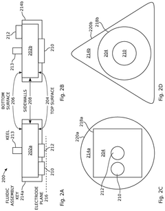
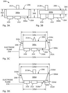
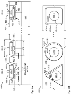
Encapsulated light emitting diodes for selective fluidic assembly
PatentActiveUS12119432B2
Innovation
- The use of partially encapsulated semiconductor-based inorganic micro-LEDs with a patternable polymer encapsulant that protects the LEDs from collisions and optimizes their shape for efficient assembly, allowing for higher speed and yield while preventing defects, and enabling precise alignment of LED colors on a display substrate.
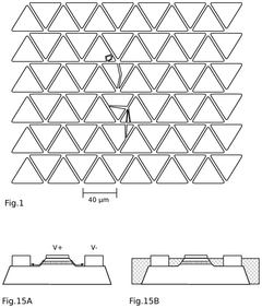
Device for self-assembling semiconductor light-emitting diodes magnets in a plurality of rows
PatentActiveUS11804384B2
Innovation
- A self-assembly device utilizing an electric field and magnetic field to guide semiconductor light-emitting diodes onto a substrate, featuring a chip supply part with a controller that moves in predetermined paths to ensure uniform distribution and positioning, thereby shortening assembly time and improving production efficiency.


Manufacturing Process Comparison
The manufacturing processes for OLED and MicroLED displays represent fundamentally different approaches to creating self-emissive display technologies. OLED manufacturing has matured significantly over the past decade, with two primary production methods: evaporation-based processes for small molecule OLEDs and solution-based printing for polymer OLEDs. The evaporation process involves depositing organic materials in vacuum chambers through precisely controlled thermal evaporation, requiring complex shadow masks for RGB patterning. This process faces challenges with scaling to larger substrates while maintaining pixel precision.
Solution-based OLED manufacturing employs inkjet printing techniques that offer potential cost advantages for larger displays but continues to struggle with achieving the color purity and lifetime performance of evaporation methods. Both approaches require stringent environmental controls, as organic materials are highly sensitive to oxygen and moisture contamination.
MicroLED manufacturing, by contrast, involves fundamentally different semiconductor fabrication techniques derived from traditional LED production. The process begins with epitaxial growth of inorganic semiconductor materials (typically GaN for blue and green, AlInGaP for red) on sapphire or silicon substrates. These wafers undergo standard semiconductor processing steps including photolithography, etching, and metallization to create individual LED structures at the microscale.
The most challenging aspect of MicroLED production is the mass transfer process, where millions of tiny LED chips must be precisely picked and placed onto the display backplane. Several approaches have emerged, including stamp transfer, laser transfer, and fluid-assisted assembly, each with varying degrees of throughput, placement accuracy, and yield rates.
OLED manufacturing benefits from established production lines and economies of scale, particularly for smartphone-sized displays. However, MicroLED offers potentially simpler device structures with fewer layers and greater material stability. The inorganic nature of MicroLEDs eliminates the need for the hermetic sealing and moisture barriers essential to OLED longevity.
Yield management represents a critical difference between the technologies. OLED manufacturing yields are primarily affected by particle contamination and thin-film uniformity issues. MicroLED yields face the compound challenge of both LED chip production yields and transfer process yields, where even 99.99% accuracy would result in thousands of defects in a 4K display, necessitating sophisticated repair mechanisms.
Cost structures also differ significantly, with OLED manufacturing being material-cost intensive while MicroLED costs are currently dominated by equipment investment and process complexity. As MicroLED manufacturing scales and matures, the inherent material advantages may eventually enable more cost-effective production for certain display applications.
Energy Efficiency and Sustainability Factors
Energy efficiency represents a critical differentiator in the evolution of display technologies, particularly when comparing OLED and MicroLED semiconductor channel structures. OLED displays operate on an emissive principle where organic compounds emit light when electricity passes through them, eliminating the need for backlighting. This fundamental architecture grants OLEDs inherent energy advantages in displaying dark content, as individual pixels can be completely turned off, consuming zero power for black areas.
MicroLED technology, while sharing the emissive display principle, utilizes inorganic gallium nitride (GaN) semiconductor materials that demonstrate superior energy conversion efficiency. Recent laboratory measurements indicate that MicroLED structures can achieve theoretical efficiency ratings 30-40% higher than current OLED implementations, particularly at higher brightness levels where OLED efficiency tends to degrade.
Power consumption patterns reveal significant differences between these technologies. OLED displays exhibit variable power consumption heavily dependent on content brightness, with exponential increases when displaying predominantly white or bright content. Conversely, MicroLED maintains more consistent power efficiency across varying brightness levels, offering substantial energy savings in high-brightness applications such as outdoor displays or automotive implementations.
From a manufacturing sustainability perspective, OLED production currently involves several environmentally challenging processes, including the use of rare earth materials and organic solvents that present disposal challenges. The shorter lifespan of organic materials also contributes to higher replacement rates and associated environmental impacts. MicroLED manufacturing, while still evolving toward mass production, utilizes more stable inorganic materials with potentially longer operational lifespans, though it currently requires more energy-intensive fabrication processes.
Heat generation and dissipation characteristics further differentiate these technologies. OLED structures generate more heat during operation, particularly at high brightness, requiring additional thermal management solutions that impact overall system efficiency. MicroLED's superior thermal properties enable more efficient operation in confined spaces and reduce cooling requirements, contributing to system-level energy savings in integrated applications.
Looking toward future developments, both technologies show promising sustainability roadmaps. OLED research focuses on phosphorescent and TADF (Thermally Activated Delayed Fluorescence) materials to improve quantum efficiency, while MicroLED development targets improved manufacturing yields and transfer processes to reduce production energy requirements. The semiconductor channel structure evolution in both technologies continues to prioritize reduced operating voltages and improved current distribution, factors that will determine their comparative sustainability profiles in next-generation display implementations.
Unlock deeper insights with PatSnap Eureka Quick Research — get a full tech report to explore trends and direct your research. Try now!
Generate Your Research Report Instantly with AI Agent
Supercharge your innovation with PatSnap Eureka AI Agent Platform!