

Optimize Atomic Force Microscopy For Advanced Semiconductor Analysis — Tactics
SEP 19, 202510 MIN READ
Generate Your Research Report Instantly with AI Agent
Patsnap Eureka helps you evaluate technical feasibility & market potential.
AFM Technology Background and Objectives
Atomic Force Microscopy (AFM) has evolved significantly since its invention in 1986 by Gerd Binnig, Calvin Quate, and Christoph Gerber. This scanning probe microscopy technique has become an indispensable tool in semiconductor analysis, offering nanoscale resolution capabilities that are crucial for modern semiconductor manufacturing processes. The technology operates by measuring forces between a sharp probe and sample surface, providing three-dimensional topographical imaging with unprecedented precision.
The semiconductor industry's relentless pursuit of Moore's Law has driven AFM technology development, as feature sizes continue to shrink below 5nm in advanced nodes. Traditional optical and electron microscopy techniques face fundamental limitations at these scales, positioning AFM as a critical metrology solution. The evolution of AFM has seen significant improvements in resolution, scanning speed, and data processing capabilities, enabling its application across various stages of semiconductor development and manufacturing.
Current AFM technology faces several limitations when applied to advanced semiconductor analysis. These include throughput constraints, challenges in measuring high-aspect-ratio structures, and difficulties in characterizing buried interfaces and subsurface features. Additionally, the integration of AFM into automated semiconductor production lines remains challenging due to speed limitations and complex sample preparation requirements.
The primary objective of optimizing AFM for advanced semiconductor analysis is to overcome these limitations while enhancing measurement accuracy, repeatability, and throughput. Specific goals include achieving sub-nanometer resolution consistently across large sample areas, reducing scan times to match production requirements, and developing specialized probes for characterizing complex 3D semiconductor structures such as FinFETs, GAA transistors, and advanced packaging solutions.
Another critical objective is the development of non-destructive subsurface imaging capabilities to analyze buried interfaces and defects without compromising sample integrity. This requires innovations in both hardware design and signal processing algorithms to extract meaningful data from complex interactions between the probe and multilayered semiconductor structures.
Data integration represents another key goal, with efforts focused on seamlessly incorporating AFM measurements into comprehensive semiconductor metrology frameworks. This includes developing standardized data formats and analysis protocols that enable correlation between AFM results and data from complementary techniques such as scanning electron microscopy (SEM) and transmission electron microscopy (TEM).
The optimization of AFM technology also aims to address emerging challenges in semiconductor manufacturing, including the characterization of novel materials like 2D semiconductors, high-k dielectrics, and advanced interconnect structures. As the industry moves toward heterogeneous integration and advanced packaging, AFM must evolve to provide critical dimensional measurements and defect analysis across increasingly complex architectures.
Semiconductor Industry Demand Analysis
The semiconductor industry's demand for advanced metrology and characterization tools has been growing exponentially with the continuous miniaturization of semiconductor devices. As process nodes shrink below 5nm and approach 3nm and beyond, traditional inspection and measurement techniques face significant limitations in resolution, accuracy, and throughput. Atomic Force Microscopy (AFM) has emerged as a critical tool for semiconductor analysis due to its ability to provide three-dimensional surface topography with sub-nanometer resolution without damaging sensitive structures.
Market research indicates that the global semiconductor metrology and inspection equipment market is projected to reach $8.6 billion by 2025, with AFM systems representing a significant growth segment. This expansion is primarily driven by the increasing complexity of semiconductor architectures, including 3D NAND, FinFETs, Gate-All-Around FETs, and heterogeneous integration technologies that require precise dimensional measurements and defect characterization.
Leading semiconductor manufacturers are specifically demanding AFM solutions with enhanced capabilities for critical dimension (CD) measurements, sidewall angle determination, and sub-surface imaging. The industry requires AFM systems that can operate at higher throughput rates while maintaining nanometer-scale precision to keep pace with high-volume manufacturing environments. Current AFM systems typically process 5-10 wafers per hour, whereas the industry target is 15-20 wafers per hour for in-line metrology applications.
Another significant market driver is the growing need for non-destructive analysis of advanced packaging technologies such as through-silicon vias (TSVs), micro-bumps, and redistribution layers. These structures require precise dimensional control and defect detection capabilities that only advanced AFM systems can provide. Industry surveys indicate that over 70% of semiconductor manufacturers consider AFM essential for their advanced packaging development and quality control processes.
The demand for AFM in failure analysis applications has also increased substantially, with particular emphasis on electrical characterization capabilities such as scanning capacitance microscopy (SCM) and conductive AFM (C-AFM). These techniques enable engineers to correlate physical defects with electrical performance issues, a critical capability as device dimensions continue to shrink and new materials are introduced into semiconductor manufacturing processes.
Geographically, the strongest demand growth for advanced AFM systems comes from East Asia, particularly Taiwan, South Korea, and China, where major semiconductor manufacturing facilities are concentrated. North American and European markets show steady demand primarily driven by research and development activities and specialized semiconductor production facilities focusing on emerging technologies.
Current AFM Capabilities and Technical Challenges
Atomic Force Microscopy (AFM) has evolved into a critical tool for semiconductor analysis, offering nanoscale imaging capabilities essential for modern chip development. Current AFM systems can achieve sub-nanometer resolution in optimal conditions, enabling detailed surface topography mapping of semiconductor structures. The technique excels in non-destructive characterization of features such as transistor gates, interconnects, and thin films without requiring vacuum conditions or complex sample preparation.
Standard AFM capabilities now include multiple imaging modes such as contact, tapping, and non-contact modes, each offering different trade-offs between resolution and sample preservation. Advanced systems incorporate phase imaging for material contrast detection and force spectroscopy for mechanical property measurements. Recent developments have integrated electrical measurement capabilities, allowing for simultaneous topographical and electrical characterization through techniques like conductive AFM (C-AFM) and Kelvin probe force microscopy (KPFM).
Despite these advancements, significant technical challenges persist when applying AFM to cutting-edge semiconductor analysis. The increasing complexity of 3D semiconductor architectures with high aspect ratio features presents accessibility issues for conventional AFM probes. Current tip geometries struggle to accurately image deep trenches and vertical sidewalls common in advanced node technologies, resulting in imaging artifacts and incomplete data collection.
Throughput limitations represent another major challenge, as traditional AFM remains relatively slow compared to other analytical techniques. Typical scan rates of 1-2 Hz per line are insufficient for high-volume manufacturing environments, where rapid feedback is essential. This speed constraint becomes particularly problematic when mapping larger areas or when statistical sampling is required across wafers.
Probe wear and contamination issues significantly impact measurement consistency and reliability. Silicon and silicon nitride tips commonly used in AFM gradually degrade during scanning, altering their geometry and affecting measurement accuracy. This degradation is accelerated when imaging hard semiconductor materials or when operating in contact mode, necessitating frequent tip replacement and recalibration.
Environmental sensitivity poses additional challenges, as thermal drift and vibration can compromise measurement precision. Even minor temperature fluctuations can cause dimensional changes that affect nanoscale measurements. Similarly, acoustic and mechanical vibrations from the surrounding environment can introduce noise and artifacts, particularly problematic for the sub-nanometer resolution required in advanced semiconductor analysis.
Data interpretation complexity has increased with semiconductor feature miniaturization. Distinguishing between actual device features and measurement artifacts requires sophisticated algorithms and expertise. The massive datasets generated by high-resolution AFM scans across multiple sample areas demand advanced data processing capabilities and standardized analysis protocols that are not yet fully developed for semiconductor-specific applications.
State-of-the-Art AFM Optimization Techniques
01 Probe and cantilever optimization
Optimization of atomic force microscopy (AFM) probes and cantilevers is crucial for improving measurement accuracy and resolution. This includes modifications to probe geometry, cantilever design, and material selection to enhance sensitivity and reduce noise. Advanced fabrication techniques allow for customized probe tips with specific properties tailored to different sample types and measurement conditions.- Probe and cantilever optimization: Optimization of atomic force microscopy (AFM) probes and cantilevers is crucial for improving measurement accuracy and resolution. This includes modifications to probe geometry, cantilever design, and material selection to enhance sensitivity and reduce noise. Advanced fabrication techniques allow for customized probe tips with specific properties tailored to different sample types and measurement conditions.
- Feedback control and signal processing: Advanced feedback control systems and signal processing algorithms are essential for optimizing AFM performance. These systems help maintain constant tip-sample interaction forces, reduce artifacts, and improve image quality. Real-time data processing techniques enable noise reduction, drift compensation, and enhanced resolution, allowing for more accurate measurements of surface topography and mechanical properties.
- Environmental and operational parameter control: Controlling environmental and operational parameters significantly impacts AFM measurement quality. This includes temperature stabilization, vibration isolation, humidity control, and optimization of scanning parameters such as scan rate and set point force. Creating optimal measurement conditions minimizes thermal drift, reduces noise, and improves reproducibility of results across different samples and experimental conditions.
- Advanced imaging modes and techniques: Development of specialized imaging modes enhances the capabilities of atomic force microscopy. These include tapping mode, non-contact mode, force spectroscopy, and multifrequency techniques that provide additional information about sample properties. Advanced techniques allow for simultaneous measurement of topography, mechanical, electrical, and magnetic properties, expanding the range of applications for AFM in materials science and biology.
- Sample preparation and positioning systems: Optimization of sample preparation methods and positioning systems improves measurement accuracy and efficiency. This includes development of sample holders, automated positioning stages, and alignment systems that enable precise control of the sample relative to the probe. Advanced sample preparation techniques help preserve sample integrity while facilitating access to regions of interest, particularly important for biological samples and nanomaterials.
02 Feedback control and signal processing techniques
Advanced feedback control systems and signal processing algorithms significantly improve AFM performance. These techniques include real-time error correction, adaptive scanning parameters, and noise filtering methods that enhance image quality and measurement precision. Digital signal processing techniques help extract meaningful data from raw measurements and compensate for environmental disturbances during scanning operations.Expand Specific Solutions03 Environmental and vibration control systems
Controlling the measurement environment is essential for high-resolution AFM imaging. This includes vibration isolation platforms, temperature stabilization systems, and acoustic shielding to minimize external disturbances. Advanced environmental chambers allow for precise control of humidity, temperature, and atmospheric composition during measurements, enabling more stable and reproducible results.Expand Specific Solutions04 High-speed and dynamic AFM techniques
Innovations in high-speed and dynamic AFM enable faster scanning rates while maintaining resolution. These techniques include resonant scanning methods, multi-frequency excitation, and specialized hardware for rapid data acquisition. Dynamic measurement modes allow for real-time observation of fast processes and time-dependent phenomena at the nanoscale, expanding the application range of AFM technology.Expand Specific Solutions05 Sample preparation and positioning systems
Precise sample preparation and positioning systems are critical for AFM optimization. This includes advanced sample holders, automated alignment mechanisms, and multi-axis positioning stages with nanometer precision. Specialized sample preparation protocols ensure optimal surface conditions for different sample types, while automated positioning systems enable precise targeting of regions of interest and reproducible measurements across multiple samples.Expand Specific Solutions
Leading AFM Equipment Manufacturers and Research Institutions
The Atomic Force Microscopy (AFM) market for semiconductor analysis is currently in a growth phase, with increasing demand driven by miniaturization trends in semiconductor manufacturing. The global market is estimated to reach approximately $1 billion by 2025, with a CAGR of 6-8%. Leading players include established research institutions like IMEC and CSIC alongside major corporations such as IBM, Applied Materials, and GlobalFoundries. The competitive landscape shows a mix of specialized AFM equipment manufacturers (Actoprobe, Xallent, Primenano) and diversified semiconductor equipment providers (Veeco Instruments, FEI). Technical maturity varies significantly, with advanced capabilities emerging from collaborations between academic institutions (McGill University, TU Munich) and industry leaders, particularly in areas of high-resolution imaging, electrical property measurement, and integration with other analytical techniques.
International Business Machines Corp.
Technical Solution: IBM has developed advanced AFM techniques specifically for semiconductor analysis, including their PrimeNano AFM platform that integrates with their semiconductor manufacturing processes. Their approach combines traditional AFM with specialized probes and machine learning algorithms to enhance imaging resolution down to sub-nanometer levels. IBM's AFM optimization includes the implementation of frequency-modulated AFM (FM-AFM) techniques that allow for non-destructive characterization of semiconductor surfaces with atomic resolution. They've also pioneered the integration of AFM with other analytical techniques such as Raman spectroscopy and infrared spectroscopy for comprehensive material analysis. IBM's recent developments include high-speed AFM systems capable of real-time imaging of dynamic processes on semiconductor surfaces, crucial for understanding defect formation and propagation during manufacturing processes.
Strengths: IBM's integration of AI and machine learning with AFM technology enables automated defect detection and classification, significantly reducing analysis time. Their multi-modal approach combining different measurement techniques provides comprehensive material characterization. Weaknesses: Their systems tend to be highly specialized and expensive, limiting widespread adoption. The complexity of their integrated systems requires specialized training and expertise to operate effectively.
GLOBALFOUNDRIES, Inc.
Technical Solution: GLOBALFOUNDRIES has developed proprietary AFM optimization techniques specifically tailored for their advanced semiconductor manufacturing processes. Their approach focuses on in-line AFM integration within the fabrication workflow, allowing for real-time monitoring and quality control. The company has implemented specialized probe technologies with enhanced durability and sensitivity, designed to withstand the harsh chemical environments present in semiconductor processing. GLOBALFOUNDRIES' AFM systems incorporate advanced vibration isolation systems and temperature control mechanisms to achieve sub-nanometer resolution even in production environments. They've also developed custom software algorithms for automated defect recognition and classification, significantly reducing the time required for analysis. Their latest innovation includes the implementation of high-speed scanning capabilities that enable throughput rates compatible with production-line requirements while maintaining the necessary resolution for advanced node technologies.
Strengths: Their AFM systems are specifically optimized for semiconductor manufacturing environments, with robust designs suitable for production use. The integration with manufacturing workflow enables real-time process control and faster response to defects. Weaknesses: The specialized nature of their systems may limit flexibility for research applications. Their focus on production environments sometimes comes at the cost of ultimate resolution capabilities compared to pure research-oriented systems.
Critical Patents and Innovations in AFM Semiconductor Analysis
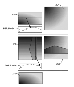
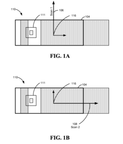
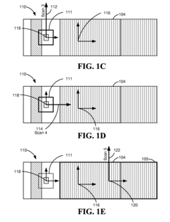
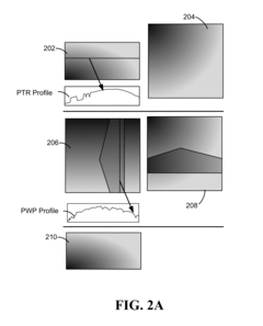
Advanced atomic force microscopy scanning for obtaining a true shape
PatentInactiveUS20130081159A1
Innovation
- The Advanced Pole tip recession and Perpendicular writer protrusion (APP) method involves performing multiple scans at different angles and positions, using image correction techniques such as true 3D image flattening and image subtraction to correct for scanner bow, system drift, and localized feature shape errors, ensuring accurate topography measurement.
Method and apparatus for performing atomic force microscopy measurements
PatentInactiveEP1237161A3
Innovation
- A method and apparatus for performing AFM measurements using a modulated force profile, allowing the probe to remain in contact with the sample while changing force levels periodically, enabling simultaneous electrical and topographical data collection without constant high force, using a force profile with defined intervals for high and low force levels and corresponding speed profiles.


Integration with Complementary Metrology Methods
The integration of Atomic Force Microscopy (AFM) with complementary metrology methods represents a critical advancement in semiconductor analysis capabilities. By combining AFM with techniques such as scanning electron microscopy (SEM), transmission electron microscopy (TEM), optical metrology, and X-ray analysis, researchers and engineers can obtain comprehensive multi-dimensional data that significantly enhances characterization accuracy and efficiency.
Cross-correlation between AFM and SEM/TEM provides particularly valuable insights, as AFM delivers superior vertical resolution while electron microscopy excels in lateral imaging and material contrast. This synergistic approach enables precise three-dimensional reconstruction of semiconductor features with nanometer-scale accuracy, critical for advanced node process development.
Optical metrology integration, including ellipsometry and reflectometry, complements AFM by providing rapid, large-area measurements that can guide more targeted AFM analysis. This combination optimizes workflow efficiency by allowing optical techniques to identify regions of interest for subsequent high-resolution AFM investigation, reducing overall measurement time while maintaining comprehensive coverage.
X-ray techniques such as X-ray photoelectron spectroscopy (XPS) and X-ray diffraction (XRD) paired with AFM create powerful analytical platforms that correlate topographical information with chemical composition and crystalline structure. This integration is particularly valuable for analyzing complex semiconductor materials and interfaces where both physical and chemical properties significantly impact device performance.
Recent developments in correlative microscopy platforms have introduced automated stage navigation and coordinate mapping systems that enable seamless transitions between different measurement techniques. These systems maintain precise sample positioning and orientation, facilitating direct comparison of data acquired from identical sample locations across multiple instruments.
Data fusion algorithms represent another frontier in integrated metrology, combining inputs from various techniques to generate comprehensive analytical models. Machine learning approaches increasingly play a role in these systems, identifying patterns and correlations across multi-technique datasets that might otherwise remain undetected through conventional analysis methods.
The implementation of standardized data formats and analysis protocols further enhances integration capabilities, allowing for more efficient data sharing between different metrology platforms. This standardization supports comprehensive semiconductor process control by enabling holistic analysis of manufacturing variations across multiple physical and chemical parameters.
Cleanroom Compatibility and Contamination Control
Cleanroom compatibility represents a critical consideration when implementing Atomic Force Microscopy (AFM) in advanced semiconductor analysis environments. Semiconductor fabrication facilities maintain stringent cleanliness standards, typically operating at ISO Class 3-5 (formerly Class 1-100) to prevent yield-reducing contamination. AFM systems deployed in these environments must adhere to these standards without compromising measurement accuracy or facility cleanliness.
Modern AFM systems designed for semiconductor applications incorporate materials and components specifically selected for cleanroom compatibility. This includes non-outgassing materials, stainless steel or anodized aluminum construction, and specialized coatings that minimize particle generation. Manufacturers like Bruker, Park Systems, and Keysight Technologies have developed dedicated semiconductor AFM platforms with cleanroom-certified components and sealed electronics compartments to prevent contamination release.
Contamination control strategies for AFM in semiconductor environments operate at multiple levels. At the system level, AFM instruments employ HEPA or ULPA filtered airflow systems to maintain positive pressure within critical components, preventing ambient particles from entering measurement chambers. Vibration isolation systems, essential for high-resolution imaging, are designed with cleanroom-compatible materials and sealed mechanisms to prevent particle generation during operation.
Sample handling represents another critical contamination vector. Advanced semiconductor AFM systems incorporate automated sample loading mechanisms that minimize human interaction and potential contamination. These systems often feature cassette-to-cassette handling compatible with Front Opening Unified Pods (FOUPs) and Standard Mechanical Interface (SMIF) pods used in semiconductor manufacturing lines, maintaining the sample's clean environment throughout the measurement process.
Maintenance protocols for cleanroom AFM systems require specialized procedures to prevent contamination introduction. This includes regular cleaning with semiconductor-grade solvents, scheduled replacement of filters and seals, and comprehensive training for operators on cleanroom protocols. Some facilities implement remote operation capabilities, allowing engineers to control AFM systems from outside the cleanroom, further reducing contamination risks associated with human presence.
Monitoring and verification of cleanroom compatibility involves regular particle counting around AFM systems during operation, verification of material outgassing characteristics, and contamination testing of samples before and after AFM analysis. Advanced facilities employ real-time monitoring systems that can detect contamination events and automatically halt operations if cleanliness thresholds are exceeded.
The integration of these contamination control strategies enables AFM to serve as a powerful analytical tool in semiconductor manufacturing environments without compromising the stringent cleanliness requirements essential for advanced node production.
Unlock deeper insights with Patsnap Eureka Quick Research — get a full tech report to explore trends and direct your research. Try now!
Generate Your Research Report Instantly with AI Agent
Supercharge your innovation with Patsnap Eureka AI Agent Platform!