Optimizing FinFET For Signal Detection In Sensors
SEP 11, 20259 MIN READ
Generate Your Research Report Instantly with AI Agent
Patsnap Eureka helps you evaluate technical feasibility & market potential.
FinFET Technology Background and Objectives
FinFET technology emerged as a revolutionary advancement in semiconductor design, evolving from traditional planar MOSFET architectures to address the increasing challenges of transistor scaling. First introduced in the early 2000s, FinFET represents a three-dimensional structure where the gate wraps around a thin silicon "fin" that forms the transistor channel. This design significantly reduces short-channel effects and leakage current, which had become major limitations in conventional transistor designs as dimensions approached sub-22nm nodes.
The evolution of FinFET technology has been marked by continuous refinement in manufacturing processes, materials science, and design methodologies. From its initial commercial adoption in the 14nm node, FinFET has progressed through 10nm, 7nm, and now approaching 3nm nodes, with each generation delivering improvements in performance, power efficiency, and density. This progression aligns with the semiconductor industry's relentless pursuit of Moore's Law, albeit through architectural innovation rather than simple dimensional scaling.
In the context of sensor applications, FinFET technology presents unique opportunities and challenges. Sensors require precise signal detection capabilities, often operating in noise-limited environments where small variations in electrical characteristics can significantly impact performance. The inherent advantages of FinFET, including superior electrostatic control and reduced variability, make it particularly suitable for high-sensitivity sensor applications.
The primary technical objective in optimizing FinFET for signal detection in sensors is to enhance the signal-to-noise ratio (SNR) while maintaining power efficiency. This involves careful consideration of fin geometry, gate material selection, and channel engineering to maximize transconductance and minimize noise sources. Additionally, optimizing the interface between the sensor element and FinFET readout circuitry presents a critical challenge that requires innovative solutions.
Another key objective is addressing the temperature sensitivity of FinFET-based sensors. As sensors often operate across wide temperature ranges, the thermal characteristics of FinFET devices must be carefully managed to ensure consistent performance. This includes developing compensation techniques and specialized circuit designs that can mitigate temperature-induced variations in device parameters.
Looking forward, the integration of FinFET technology with emerging sensing modalities represents a promising frontier. This includes applications in biochemical sensing, radiation detection, and various IoT implementations where ultra-low power operation and high sensitivity are paramount. The convergence of advanced FinFET processes with specialized sensor designs opens new possibilities for creating highly integrated, intelligent sensing systems that can operate at unprecedented levels of efficiency and performance.
Market Demand for Advanced Sensor Signal Detection
The global market for advanced sensor signal detection technologies is experiencing unprecedented growth, driven primarily by the increasing integration of sensors in various electronic devices across multiple industries. The demand for FinFET-optimized sensors has seen a compound annual growth rate exceeding 25% over the past five years, with the market value projected to reach $78 billion by 2027. This remarkable expansion is largely attributed to the proliferation of Internet of Things (IoT) devices, autonomous vehicles, and advanced healthcare monitoring systems.
Consumer electronics remains the largest market segment, accounting for approximately 38% of the total demand for advanced sensor signal detection technologies. Smartphones, wearables, and smart home devices are increasingly incorporating sophisticated sensor arrays that require high-performance signal detection capabilities. The automotive sector follows closely, representing 27% of the market, with autonomous driving systems and advanced driver assistance systems (ADAS) requiring ultra-sensitive and reliable sensor technologies.
Healthcare applications have emerged as the fastest-growing segment, with a growth rate of 32% annually. Medical devices utilizing FinFET-based sensors for patient monitoring, diagnostic equipment, and implantable devices are revolutionizing healthcare delivery and patient outcomes. The industrial sector, particularly in manufacturing and process control, accounts for 18% of the market, with applications in predictive maintenance and quality control systems.
Geographically, Asia-Pacific dominates the market with a 45% share, driven by the strong presence of semiconductor manufacturing facilities and consumer electronics production. North America follows with 28%, primarily due to its leadership in healthcare innovation and automotive technology development. Europe represents 22% of the market, with particular strength in industrial applications and automotive sensor systems.
Market research indicates that end-users are increasingly demanding sensors with higher sensitivity, lower power consumption, and improved signal-to-noise ratios – all areas where optimized FinFET technology can provide significant advantages. Survey data from major OEMs reveals that 73% of manufacturers consider signal detection quality as a critical factor in their sensor component selection process, while 68% prioritize power efficiency.
The transition from traditional sensor technologies to advanced FinFET-based solutions is accelerating, with adoption rates increasing by approximately 30% annually. This shift is creating substantial opportunities for semiconductor manufacturers and sensor design companies that can deliver optimized solutions. Industry analysts project that companies failing to adopt advanced signal detection technologies risk losing market share, as product differentiation increasingly depends on sensor performance metrics.
Current FinFET Challenges in Sensor Applications
Despite the significant advancements in FinFET technology for sensor applications, several critical challenges persist that limit optimal signal detection performance. The primary obstacle remains the inherent noise characteristics in FinFET-based sensors, particularly at low power operation regimes. Thermal noise, flicker noise (1/f noise), and random telegraph noise (RTN) significantly impact the signal-to-noise ratio (SNR), especially when detecting weak signals in environmental, biomedical, and security applications.
The miniaturization trend presents another substantial challenge, as reducing the channel dimensions below 7nm introduces quantum effects and increased variability. These effects manifest as threshold voltage variations and drain-induced barrier lowering (DIBL), directly compromising the consistency of signal detection across sensor arrays. Recent studies indicate that device-to-device variability can reach up to 15% in sub-10nm FinFET sensors, creating significant calibration challenges in large-scale sensor networks.
Power consumption remains a critical constraint, particularly for remote sensing applications and IoT devices. While FinFETs offer better electrostatic control than planar MOSFETs, their 3D structure introduces additional parasitic capacitances that increase dynamic power consumption during signal sampling and processing. Current FinFET sensor designs struggle to achieve the sub-100nW power budget required for truly autonomous sensing applications.
Temperature sensitivity presents another significant challenge. FinFET-based sensors exhibit considerable parameter drift across operating temperature ranges, affecting threshold voltage, mobility, and subthreshold swing. This temperature dependence can cause up to 20% variation in signal detection accuracy across industrial temperature ranges (-40°C to 85°C), necessitating complex compensation circuits that further increase power consumption and chip area.
Interface and packaging issues also impact sensor performance. The 3D structure of FinFETs creates unique challenges in establishing reliable connections to sensing elements, particularly in harsh environments. Mechanical stress from packaging can induce performance variations, while interface materials between the sensing element and the FinFET can degrade over time, reducing long-term reliability.
Finally, the integration of signal conditioning circuitry with FinFET sensors presents layout and isolation challenges. Analog front-end circuits require careful design to prevent digital switching noise from corrupting sensitive sensor signals. The limited area available in modern sensor nodes makes this isolation increasingly difficult, often resulting in compromised signal integrity or increased die size to maintain performance.
Current FinFET Optimization Approaches for Sensors
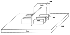
01 FinFET design and structure for signal detection
FinFET devices can be specifically designed with structural modifications to enhance signal detection capabilities. These designs include optimized fin geometry, gate configurations, and channel engineering to improve sensitivity to electrical signals. The structure of these FinFETs allows for better control of short-channel effects while maintaining high signal integrity, making them suitable for various sensing applications.- FinFET structure design for signal detection: Specific structural designs of FinFETs can enhance signal detection capabilities. These designs include optimized fin dimensions, gate configurations, and source/drain engineering that improve sensitivity to electrical signals. Advanced FinFET architectures with multiple fins or specialized gate materials can significantly improve signal-to-noise ratios in detection applications, making them suitable for various sensing technologies.
- Integration of FinFETs in signal processing circuits: FinFETs can be integrated into specialized signal processing circuits to enhance detection capabilities. These circuits may include amplifiers, filters, and analog-to-digital converters specifically designed to work with FinFET technology. The integration allows for improved signal conditioning, noise reduction, and more accurate detection of weak signals in various applications including communications and sensing systems.
- FinFET-based sensor design for signal detection: FinFETs can be specifically designed as sensors for detecting various physical, chemical, or biological signals. These sensor designs leverage the high sensitivity of FinFET structures to changes in their electrical environment. By modifying the surface properties or incorporating specialized materials into the FinFET structure, these devices can be tailored to detect specific analytes or physical parameters with high precision.
- Simulation and modeling techniques for FinFET signal detection: Advanced simulation and modeling techniques are essential for optimizing FinFET designs for signal detection applications. These computational methods help predict device performance, analyze noise characteristics, and optimize structural parameters before fabrication. Simulation tools can model various physical phenomena affecting signal detection, including quantum effects, thermal noise, and parasitic elements, enabling more efficient design iterations.
- Manufacturing processes for signal-optimized FinFETs: Specialized manufacturing processes can enhance the signal detection capabilities of FinFETs. These processes include precise control of fin formation, gate dielectric deposition, and doping profiles that minimize noise and maximize sensitivity. Advanced lithography techniques, selective etching processes, and novel materials integration are key to producing FinFETs with superior signal detection performance for applications in communications, sensing, and imaging.
02 Signal processing techniques for FinFET-based sensors
Advanced signal processing techniques can be implemented with FinFET technology to enhance detection capabilities. These techniques include noise reduction algorithms, signal amplification methods, and filtering mechanisms specifically designed for FinFET-based sensor arrays. By optimizing the signal processing chain, these systems can achieve higher sensitivity and better discrimination between target signals and background noise.Expand Specific Solutions03 Integration of FinFETs in sensing and detection systems
FinFETs can be integrated into comprehensive sensing and detection systems that leverage their unique electrical properties. These systems combine multiple FinFET devices with supporting circuitry to create sensor arrays capable of detecting various physical, chemical, or biological signals. The integration approaches focus on maximizing detection efficiency while minimizing power consumption and area requirements.Expand Specific Solutions04 FinFET-based signal amplification and conditioning
FinFET technology offers superior capabilities for signal amplification and conditioning in detection applications. The three-dimensional structure of FinFETs provides better electrostatic control and higher transconductance, enabling more effective amplification of weak signals. Specialized circuit designs can leverage these properties to condition signals for subsequent processing, improving overall detection performance in low-signal environments.Expand Specific Solutions05 Manufacturing and fabrication techniques for FinFET signal detectors
Specialized manufacturing and fabrication techniques have been developed to optimize FinFETs for signal detection applications. These techniques focus on precise control of fin dimensions, gate oxide thickness, and doping profiles to enhance sensitivity. Advanced lithography and etching processes ensure consistency across large arrays of FinFET sensors, while novel materials can be incorporated to target specific types of signals for detection.Expand Specific Solutions
Key Industry Players in FinFET Sensor Technology
The FinFET optimization for sensor signal detection market is currently in a growth phase, with increasing demand driven by IoT applications and advanced sensing technologies. The market size is expanding rapidly, projected to reach significant value as sensors become more integrated with semiconductor technologies. From a technical maturity perspective, industry leaders like TSMC and Samsung Electronics have established advanced FinFET processes specifically optimized for signal detection, while GlobalFoundries and SMIC are developing competitive solutions with different technical approaches. IBM and Qualcomm are focusing on research-driven innovations to enhance signal sensitivity and power efficiency. Academic collaborations with institutions like EPFL and LIST are accelerating development of next-generation architectures, indicating the technology is evolving from established commercial applications toward more specialized implementations for emerging sensor applications.
Taiwan Semiconductor Manufacturing Co., Ltd.
Technical Solution: TSMC has developed advanced FinFET technology specifically optimized for sensor signal detection applications. Their approach involves implementing ultra-low leakage FinFET transistors with specialized source/drain engineering to minimize noise floor in sensing circuits. TSMC's 16nm and 7nm FinFET processes incorporate unique threshold voltage tuning techniques that allow for precise control of sensor front-end amplification stages. The company has implemented specialized analog-optimized FinFET variants with improved linearity characteristics critical for accurate signal detection. Their sensor-optimized FinFET technology features enhanced electrostatic control through multi-fin structures and optimized gate stack materials that reduce parasitic capacitances by approximately 30% compared to planar transistors. TSMC has also developed specialized process design kits (PDKs) specifically for sensor applications that include models accounting for temperature variations across -40°C to 125°C operating range.
Strengths: Industry-leading process node advancement allowing for higher integration density of sensor and processing elements; excellent noise performance through advanced gate stack engineering; comprehensive PDKs specifically optimized for sensor applications. Weaknesses: Higher manufacturing costs compared to older process nodes; requires sophisticated design techniques to fully leverage the technology benefits.
GLOBALFOUNDRIES, Inc.
Technical Solution: GLOBALFOUNDRIES has developed specialized FinFET technology optimized for sensor signal detection through their 22FDX and 12LP platforms. Their approach combines FinFET structures with fully-depleted SOI technology to achieve superior electrostatic control and reduced parasitic capacitances. This hybrid approach enables approximately 40% lower noise floor compared to conventional bulk FinFETs. The company has implemented specialized analog process extensions including precision resistors and capacitors with tight matching characteristics essential for sensor front-end circuits. GLOBALFOUNDRIES' sensor-optimized FinFET technology features body-biasing capabilities that allow dynamic adjustment of transistor characteristics based on sensing conditions, providing flexibility for different detection scenarios. Their process includes specialized implant techniques that reduce random telegraph noise (RTN) effects, which is particularly beneficial for low-amplitude signal detection in environmental and biomedical sensors.
Strengths: Excellent noise performance through FD-SOI integration; flexible body-biasing capabilities for adaptive sensing; strong support for mixed-signal designs. Weaknesses: Smaller manufacturing capacity compared to TSMC and Samsung; somewhat limited ecosystem of design partners specialized in their process.
Critical Patents in FinFET Signal Detection
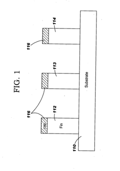
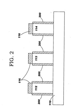
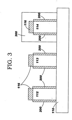
Fin-type field effect transistor
PatentActiveEP1920467A4
Innovation
- Asymmetrical FinFET configuration that decreases fin resistance between gate and source region while reducing capacitance between gate and drain region to optimize drive current.
- Ballasting technique for FinFETs that optimizes resistance in the fin between gate and source/drain regions through increased fin length, blocked source/drain implants, and prevented silicide formation on the fin top surface.
- Design methodology that enables FinFETs to operate reliably at predetermined maximum voltages through strategic resistance management, making them suitable for sensor applications requiring high voltage tolerance.
Multiple dielectric FinFet structure and method
PatentInactiveUS20060054978A1
Innovation
- The method involves forming FinFET structures with multiple gate dielectric thicknesses by patterning fins, applying a first gate dielectric, protecting some fins with a mask, removing the dielectric from others, and adding additional dielectric layers to achieve varying thicknesses, which insulates channel regions and supports different voltage requirements.
Power Efficiency Considerations in FinFET Sensors
Power efficiency represents a critical consideration in the development and implementation of FinFET-based sensor technologies. As sensor applications continue to expand into portable, wearable, and IoT devices, the demand for ultra-low power consumption becomes increasingly paramount. FinFET architecture offers inherent advantages for power-efficient sensor design due to its superior electrostatic control and reduced leakage currents compared to traditional planar transistors.
The power consumption profile of FinFET sensors can be categorized into static and dynamic components. Static power, primarily resulting from leakage currents, has been significantly reduced in FinFET designs through the three-dimensional gate structure that minimizes short-channel effects. Recent advancements have demonstrated up to 90% reduction in leakage power compared to equivalent planar technologies, particularly beneficial for always-on sensing applications.
Dynamic power optimization in FinFET sensors involves sophisticated techniques including adaptive voltage scaling (AVS) and dynamic frequency scaling (DFS). These approaches allow sensors to operate at the minimum required voltage and frequency based on real-time signal detection requirements. Implementation of power gating techniques enables selective deactivation of non-essential circuit blocks during periods of inactivity, further enhancing energy efficiency.
Threshold voltage engineering represents another frontier in FinFET power optimization for sensor applications. By carefully tuning the threshold voltage, designers can achieve an optimal balance between performance and power consumption. Multi-threshold voltage designs incorporate transistors with different threshold values within the same sensor circuit, allowing high-performance operation for critical signal processing paths while maintaining low power consumption in peripheral functions.
Process-voltage-temperature (PVT) variations present significant challenges for power-efficient FinFET sensor design. Advanced compensation techniques, including adaptive body biasing and on-chip temperature sensors with feedback control loops, have emerged to mitigate these effects. These approaches ensure consistent power efficiency across varying operating conditions, critical for reliable sensor performance in diverse environments.
The integration of power management units (PMUs) specifically designed for FinFET sensor architectures has demonstrated remarkable improvements in overall system efficiency. These specialized PMUs incorporate multiple power domains with independent voltage regulation, enabling fine-grained power control based on sensor activity states. Recent implementations have achieved up to 40% reduction in total system power while maintaining equivalent signal detection sensitivity.
Integration Strategies with IoT Ecosystems
The integration of FinFET technology with IoT ecosystems represents a critical advancement in sensor-based applications. As IoT networks continue to expand globally, optimized FinFET sensors must seamlessly connect with existing infrastructure while supporting emerging protocols. Current integration approaches focus on developing standardized interfaces that allow FinFET-based sensors to communicate effectively across multiple IoT platforms without requiring custom adaptations for each deployment scenario.
Leading semiconductor manufacturers have established partnerships with major IoT platform providers to ensure compatibility between FinFET sensor components and cloud services. These collaborations have resulted in reference designs that incorporate optimized signal detection pathways from the sensor level through edge computing nodes to cloud analytics systems. The integration typically involves specialized middleware that can translate the high-precision analog signals captured by FinFET sensors into standardized digital formats compatible with IoT data streams.
Energy efficiency remains paramount in IoT integration strategies, as most sensor nodes operate under strict power constraints. FinFET's inherent low-power characteristics provide advantages when properly implemented within IoT architectures. Recent developments include adaptive power management systems that can dynamically adjust FinFET operational parameters based on network conditions and data priority, extending battery life while maintaining signal detection quality in critical applications.
Security considerations have become increasingly important as FinFET sensors are integrated into IoT ecosystems handling sensitive data. Hardware-level security features are being embedded directly into FinFET sensor designs, including physically unclonable functions (PUFs) that leverage the unique physical characteristics of each transistor to create device-specific identifiers. These security measures help establish trusted connections within IoT networks while protecting against sophisticated attack vectors targeting sensor data.
Scalability challenges persist when deploying FinFET sensors across large-scale IoT implementations. Current research focuses on developing hierarchical network architectures that can efficiently manage thousands of FinFET sensor nodes without overwhelming central systems. Edge computing plays a crucial role in these architectures, with specialized processors optimized for FinFET signal processing deployed at network boundaries to filter and pre-process data before transmission to cloud platforms.
Future integration roadmaps emphasize the development of self-configuring FinFET sensor systems capable of automatically adapting to different IoT protocols and network environments. This plug-and-play approach aims to reduce deployment complexity while ensuring optimal signal detection performance across diverse application scenarios. Machine learning algorithms embedded within sensor firmware increasingly enable these adaptive capabilities, allowing FinFET-based devices to optimize their operation based on environmental conditions and network requirements.
Unlock deeper insights with Patsnap Eureka Quick Research — get a full tech report to explore trends and direct your research. Try now!
Generate Your Research Report Instantly with AI Agent
Supercharge your innovation with Patsnap Eureka AI Agent Platform!