PTFE and Its Role in Cutting‑Edge Semiconductor Technology
JUN 27, 20259 MIN READ
Generate Your Research Report Instantly with AI Agent
Patsnap Eureka helps you evaluate technical feasibility & market potential.
PTFE in Semiconductors: Background and Objectives
Polytetrafluoroethylene (PTFE), commonly known as Teflon, has emerged as a critical material in cutting-edge semiconductor technology. Its unique properties, including exceptional chemical resistance, low dielectric constant, and high thermal stability, have positioned PTFE as an indispensable component in various semiconductor applications.
The semiconductor industry has witnessed rapid advancements in recent decades, driven by the relentless pursuit of miniaturization and increased performance. As chip manufacturers push the boundaries of Moore's Law, they face numerous challenges in maintaining device reliability and performance at increasingly smaller scales. PTFE has played a crucial role in addressing these challenges, particularly in areas such as insulation, packaging, and contamination control.
The evolution of PTFE's use in semiconductors can be traced back to the 1960s when it was first introduced as a coating material for electronic components. Since then, its applications have expanded significantly, encompassing a wide range of semiconductor manufacturing processes and end-products. The material's ability to withstand high temperatures and resist chemical degradation has made it particularly valuable in the harsh environments typical of semiconductor fabrication.
In recent years, the demand for PTFE in the semiconductor industry has grown exponentially, driven by the increasing complexity of chip designs and the need for more sophisticated manufacturing techniques. The material's low friction properties have proven essential in the development of advanced lithography systems, while its excellent insulating characteristics have facilitated the creation of high-performance interconnects and packaging solutions.
As the semiconductor industry continues to evolve, new challenges emerge that require innovative materials and technologies. PTFE is expected to play an even more significant role in addressing these challenges, with ongoing research focused on enhancing its properties and expanding its applications. The development of PTFE nanocomposites and the exploration of novel synthesis methods are among the key areas of investigation aimed at pushing the boundaries of semiconductor technology.
The objectives of incorporating PTFE in cutting-edge semiconductor technology are multifaceted. Primarily, researchers and industry professionals aim to leverage PTFE's unique properties to improve device performance, reliability, and longevity. This includes enhancing thermal management, reducing signal interference, and minimizing contamination risks in increasingly complex chip architectures. Additionally, there is a strong focus on developing PTFE-based solutions that can enable the next generation of semiconductor devices, such as those required for quantum computing and advanced AI applications.
Market Analysis for PTFE in Semiconductor Industry
The global semiconductor industry has witnessed significant growth in recent years, with the market for PTFE (Polytetrafluoroethylene) playing a crucial role in this expansion. As semiconductor technologies advance, the demand for high-performance materials like PTFE continues to rise, driven by its unique properties that make it ideal for various applications in chip manufacturing processes.
The market for PTFE in the semiconductor industry is primarily fueled by the increasing complexity of integrated circuits and the need for materials that can withstand harsh chemical environments and high temperatures. PTFE's excellent dielectric properties, chemical resistance, and thermal stability make it an essential component in semiconductor fabrication equipment, wafer processing, and packaging applications.
In terms of market size, the PTFE segment within the semiconductor industry has been experiencing steady growth. This growth is attributed to the rising demand for advanced semiconductor devices in various sectors, including consumer electronics, automotive, and industrial applications. The proliferation of technologies such as 5G, artificial intelligence, and the Internet of Things (IoT) has further accelerated the need for high-performance semiconductors, consequently boosting the demand for PTFE.
Geographically, the Asia-Pacific region dominates the PTFE market in the semiconductor industry, with countries like China, Taiwan, South Korea, and Japan leading the way. This dominance is primarily due to the concentration of semiconductor manufacturing facilities in these countries. North America and Europe also represent significant markets, driven by their advanced research and development capabilities and the presence of major semiconductor companies.
The market for PTFE in the semiconductor industry is characterized by intense competition among key players. Major companies in this space are continuously investing in research and development to enhance their product offerings and maintain their market position. Additionally, there is a growing trend towards the development of eco-friendly and sustainable PTFE alternatives, in response to increasing environmental concerns and regulations.
Looking ahead, the market for PTFE in the semiconductor industry is poised for continued growth. Factors such as the ongoing miniaturization of electronic devices, the development of advanced packaging technologies, and the emergence of new applications in areas like quantum computing and neuromorphic chips are expected to drive demand for PTFE and related materials. However, challenges such as supply chain disruptions and the need for more sustainable manufacturing processes may impact market dynamics in the coming years.
Current PTFE Applications and Challenges in Semiconductors
Polytetrafluoroethylene (PTFE) has become an indispensable material in the semiconductor industry, playing a crucial role in various applications due to its unique properties. In cutting-edge semiconductor technology, PTFE is extensively used in wafer processing, chemical delivery systems, and cleanroom environments.
One of the primary applications of PTFE in semiconductor manufacturing is in chemical delivery systems. The material's exceptional chemical resistance and low reactivity make it ideal for handling corrosive and ultra-pure chemicals used in semiconductor fabrication. PTFE tubing, valves, and fittings are widely employed to transport and dispense these chemicals without contamination or degradation.
In wafer processing, PTFE-based components are utilized in various stages. For instance, PTFE-coated wafer carriers and cassettes protect delicate silicon wafers during transportation and storage. The material's non-stick properties prevent particle adhesion, reducing the risk of contamination and improving yield rates.
PTFE also finds extensive use in plasma etching and deposition processes. PTFE-based chamber liners and shields protect reactor walls from corrosive plasmas and minimize particle generation. Additionally, PTFE is used in gas distribution systems within these chambers, ensuring uniform and controlled gas flow during critical processes.
Despite its widespread adoption, PTFE faces several challenges in semiconductor applications. One significant issue is the material's tendency to cold flow or creep under stress, which can lead to seal failures in high-pressure systems. This limitation necessitates careful design considerations and regular maintenance to ensure system integrity.
Another challenge is PTFE's relatively high coefficient of thermal expansion compared to metals used in semiconductor equipment. This mismatch can cause sealing issues in applications involving temperature fluctuations, requiring innovative design solutions to maintain leak-tight connections.
The semiconductor industry's push towards smaller feature sizes and higher purity standards also presents challenges for PTFE. As process tolerances become tighter, even trace amounts of contamination from PTFE degradation or outgassing can impact device performance. This has led to ongoing research into ultra-high purity grades of PTFE and alternative fluoropolymers with enhanced stability.
Lastly, the increasing focus on sustainability in semiconductor manufacturing has raised concerns about the environmental impact of PTFE production and disposal. The industry is exploring more eco-friendly fluoropolymer alternatives and improved recycling methods for PTFE components to address these concerns.
Existing PTFE Solutions for Semiconductor Fabrication
01 PTFE manufacturing processes
Various methods for producing PTFE are described, including polymerization techniques, extrusion processes, and molding methods. These processes aim to improve the quality, efficiency, and properties of the resulting PTFE materials.- PTFE manufacturing processes: Various methods for producing PTFE are described, including polymerization techniques, extrusion processes, and molding methods. These processes aim to improve the quality, efficiency, and properties of the resulting PTFE materials.
- PTFE composite materials: PTFE is often combined with other materials to create composite structures with enhanced properties. These composites may include fillers, reinforcing agents, or other polymers to improve mechanical strength, thermal stability, or specific functional characteristics.
- Surface modification of PTFE: Techniques for modifying the surface properties of PTFE are explored, including chemical treatments, plasma treatments, and coating methods. These modifications aim to improve adhesion, wettability, or introduce specific functionalities to PTFE surfaces.
- PTFE in membrane applications: PTFE is widely used in membrane technologies for various applications such as filtration, separation, and gas diffusion. The development of PTFE membranes with specific pore sizes, structures, and surface properties is discussed for different industrial and environmental applications.
- PTFE in coating formulations: The use of PTFE in coating formulations is explored, focusing on its non-stick and low friction properties. Various methods for incorporating PTFE into coatings, as well as techniques for improving coating adhesion and durability, are discussed.
02 PTFE composite materials
PTFE is combined with other materials to create composite structures with enhanced properties. These composites may include reinforcing fibers, nanoparticles, or other polymers to improve strength, conductivity, or other specific characteristics.Expand Specific Solutions03 Surface modification of PTFE
Techniques for modifying the surface of PTFE materials are explored to enhance properties such as adhesion, wettability, or biocompatibility. These modifications may involve chemical treatments, plasma processing, or the application of coatings.Expand Specific Solutions04 PTFE in membrane technology
PTFE is utilized in the development of advanced membrane technologies for various applications, including filtration, separation, and gas diffusion. These membranes leverage PTFE's unique properties such as chemical resistance and hydrophobicity.Expand Specific Solutions05 PTFE applications in specific industries
The use of PTFE in various industrial applications is described, including automotive, electronics, medical devices, and textiles. These applications take advantage of PTFE's low friction, non-stick properties, and chemical inertness.Expand Specific Solutions
Key Players in PTFE and Semiconductor Industries
The PTFE market in semiconductor technology is in a mature growth phase, with increasing demand driven by the industry's continuous advancement. The global market size for PTFE in semiconductors is substantial, reflecting its critical role in high-performance applications. Technologically, PTFE has reached a high level of maturity, with ongoing innovations focused on enhancing its properties for specific semiconductor applications. Key players like DAIKIN INDUSTRIES, W. L. Gore & Associates, and 3M Innovative Properties are at the forefront, leveraging their extensive R&D capabilities to develop advanced PTFE formulations. Other significant contributors include Nitto Denko, AGC, and DuPont Safety & Construction, each bringing specialized expertise to the field. The competitive landscape is characterized by a mix of established chemical giants and niche players, all striving to meet the evolving demands of the semiconductor industry.
DAIKIN INDUSTRIES Ltd.
Technical Solution: Daikin Industries has developed advanced PTFE materials specifically tailored for semiconductor applications. Their OPTOOL™ DSX series utilizes a unique molecular structure that enhances the material's durability and chemical resistance[1]. This technology allows for the creation of ultra-thin PTFE films, as thin as 10 nanometers, which are crucial for advanced semiconductor manufacturing processes[2]. Daikin's PTFE formulations also incorporate nano-scale additives to improve thermal management and reduce particle generation, addressing key challenges in high-performance chip production[3]. The company has further innovated by developing plasma-resistant PTFE grades that can withstand the harsh environments in plasma etching chambers, extending the lifespan of critical semiconductor equipment components[4].
Strengths: Superior chemical resistance and thermal stability, ultra-thin film capability, and enhanced plasma resistance. Weaknesses: Higher cost compared to standard PTFE, and potential limitations in extreme high-temperature applications.
W. L. Gore & Associates, Inc.
Technical Solution: W. L. Gore & Associates has pioneered the use of expanded PTFE (ePTFE) in semiconductor manufacturing. Their GORE® PTFE Membrane technology creates a microporous structure that offers exceptional particle filtration while maintaining high gas flow rates, critical for clean room environments[5]. The company has also developed specialized PTFE-based materials for chemical mechanical planarization (CMP) processes, which provide improved planarity and reduced defectivity in wafer production[6]. Gore's advanced PTFE composites are engineered to withstand aggressive chemicals and high temperatures encountered in semiconductor wet processing, offering extended service life and reduced contamination risks[7]. Additionally, their PTFE-based sealing solutions for semiconductor equipment demonstrate superior leak-tightness and minimal outgassing, contributing to improved yield and reliability in chip manufacturing[8].
Strengths: Exceptional filtration capabilities, high chemical compatibility, and proven track record in semiconductor applications. Weaknesses: Limited customization options for some specialized processes and potentially higher initial investment costs.
Innovative PTFE Formulations for Advanced Semiconductors
Semiconductor Device and Methods of Making and Using an Enhanced Carrier to Reduce Electrostatic Discharge
PatentPendingUS20240355655A1
Innovation
- A Polytetrafluoroethylene (PTFE) coating is applied to semiconductor manufacturing boat carriers to reduce electrostatic discharge, combined with a primer layer and surface roughening to enhance adhesion and mechanical resilience, effectively blocking ESD and protecting semiconductor devices.
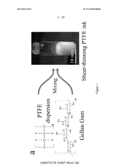
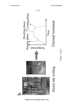
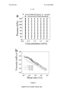
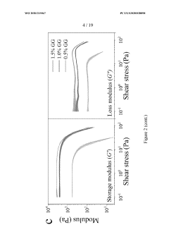
Fluoropolymer shear-thinning INKS and methods of making and using same
PatentWO2020215047A1
Innovation
- Development of shear-thinning inks comprising PTFE particles, a medium, and a shear-thinning agent like gellan gum, combined with a multistage thermal treatment process for direct ink writing, allowing for the creation of complex PTFE structures with tunable mechanical properties.
Environmental Impact of PTFE in Semiconductor Production
The use of PTFE (Polytetrafluoroethylene) in semiconductor production has raised significant environmental concerns due to its persistence and potential for bioaccumulation. PTFE is widely used in semiconductor manufacturing for its excellent chemical resistance and low friction properties, particularly in equipment components and as a coating material. However, the production and disposal of PTFE-containing materials can have substantial environmental impacts.
During the manufacturing process of PTFE, perfluorooctanoic acid (PFOA) is often used as a processing aid. PFOA is a persistent organic pollutant that has been linked to various health and environmental issues. Although many manufacturers have phased out PFOA, alternative processing aids may still pose environmental risks. The production of PTFE also involves the use of fluoropolymer precursors, which can contribute to greenhouse gas emissions if not properly managed.
In semiconductor fabrication facilities, PTFE components may degrade over time, releasing microparticles and potentially harmful chemicals into the environment. These particles can contaminate water sources and soil, posing risks to aquatic ecosystems and potentially entering the food chain. The extreme stability of PTFE means that these particles can persist in the environment for extended periods, potentially accumulating in organisms and ecosystems.
The disposal of PTFE-containing waste from semiconductor production presents another environmental challenge. Incineration of PTFE can release toxic fluorine compounds and other harmful substances into the atmosphere. Landfilling is not an ideal solution either, as PTFE does not biodegrade and can leach chemicals into groundwater over time.
To address these environmental concerns, the semiconductor industry is exploring alternatives to PTFE and implementing more sustainable practices. Some companies are investigating bio-based or recyclable fluoropolymers that offer similar properties to PTFE but with reduced environmental impact. Others are focusing on improving PTFE recycling technologies to minimize waste and reduce the need for virgin material production.
Regulatory bodies worldwide are also taking action to mitigate the environmental impact of PTFE and related compounds. Stricter regulations on the use and disposal of fluoropolymers in semiconductor production are being implemented, encouraging manufacturers to adopt more environmentally friendly alternatives and improve their waste management practices.
As the semiconductor industry continues to grow, balancing technological advancement with environmental responsibility remains a critical challenge. The ongoing research into greener alternatives and improved lifecycle management of PTFE in semiconductor production will be crucial in minimizing the environmental footprint of this essential industry.
PTFE Alternatives and Complementary Materials in Semiconductors
While PTFE has been a cornerstone material in semiconductor manufacturing, the industry's relentless pursuit of miniaturization and performance enhancement has led to the exploration of alternative and complementary materials. These materials aim to address the limitations of PTFE while maintaining or improving upon its desirable properties.
One promising alternative is perfluoroalkoxy alkane (PFA), which offers similar chemical resistance and low dielectric properties to PTFE but with improved mechanical strength and a higher continuous service temperature. PFA's enhanced thermal stability makes it suitable for more demanding semiconductor processes, particularly in high-temperature applications.
Another material gaining traction is polyetheretherketone (PEEK), known for its exceptional mechanical and thermal properties. PEEK exhibits excellent resistance to high-energy radiation, making it valuable in certain semiconductor manufacturing steps where radiation exposure is a concern. Its ability to maintain dimensional stability at elevated temperatures also contributes to its growing adoption in the industry.
Fluorinated ethylene propylene (FEP) is another fluoropolymer that complements PTFE in semiconductor applications. FEP shares many of PTFE's beneficial properties but offers improved clarity and a lower melting point, allowing for easier processing in some manufacturing scenarios.
In the realm of thin films and coatings, materials like parylene are emerging as alternatives to PTFE. Parylene coatings provide excellent barrier properties and can be applied in extremely thin, uniform layers, making them suitable for protecting sensitive semiconductor components.
For applications requiring enhanced hardness and wear resistance, ceramic materials such as aluminum nitride (AlN) and silicon carbide (SiC) are being explored. These materials offer excellent thermal conductivity and can withstand harsh chemical environments, properties that are crucial in certain semiconductor manufacturing processes.
Graphene and other two-dimensional materials are also under investigation for their potential in semiconductor technology. Their unique electronic properties and atomic-scale thickness offer intriguing possibilities for next-generation devices, although challenges in large-scale production and integration remain.
As the semiconductor industry continues to evolve, the development and integration of these alternative and complementary materials will play a crucial role in overcoming current technological barriers and enabling future innovations in chip design and manufacturing processes.
Unlock deeper insights with Patsnap Eureka Quick Research — get a full tech report to explore trends and direct your research. Try now!
Generate Your Research Report Instantly with AI Agent
Supercharge your innovation with Patsnap Eureka AI Agent Platform!