Quantum Dot Stability in Advanced Nanolithography
SEP 28, 202510 MIN READ
Generate Your Research Report Instantly with AI Agent
Patsnap Eureka helps you evaluate technical feasibility & market potential.
Quantum Dot Nanolithography Background and Objectives
Quantum dot technology has evolved significantly since its theoretical conception in the 1970s and experimental realization in the 1980s. These semiconductor nanocrystals, typically ranging from 2-10 nanometers in diameter, exhibit unique quantum confinement effects that enable precise control of their optical and electronic properties through size manipulation. The integration of quantum dots into nanolithography represents a convergence of quantum physics, materials science, and advanced manufacturing techniques that has accelerated dramatically over the past decade.
The evolution of quantum dot applications in lithography has been driven by the semiconductor industry's relentless pursuit of Moore's Law and the increasing demand for higher resolution patterning techniques. Traditional photolithography reached its fundamental diffraction limits in the early 2000s, creating an urgent need for alternative approaches capable of achieving sub-10nm feature sizes. Quantum dot nanolithography emerged as a promising candidate due to its potential for unprecedented resolution and pattern fidelity.
Recent technological advancements have focused on enhancing quantum dot stability, which remains the primary challenge limiting widespread industrial adoption. Quantum dots are inherently susceptible to oxidation, photobleaching, and aggregation, particularly under the intense energy conditions required for lithographic processes. The stability issue manifests as inconsistent pattern transfer, reduced resolution, and compromised reproducibility in manufacturing environments.
The primary objective of current research in quantum dot nanolithography is to develop robust stabilization strategies that preserve the exceptional optical and electronic properties of quantum dots while enabling their integration into high-volume manufacturing processes. This includes engineering surface passivation techniques, developing novel core-shell architectures, and creating specialized dispersion media that minimize degradation during lithographic exposure.
Secondary objectives include optimizing quantum dot composition for specific wavelength requirements, enhancing quantum yield for improved sensitivity, and developing environmentally benign synthesis methods that reduce reliance on toxic precursors. These objectives align with broader industry trends toward more sustainable and efficient nanomanufacturing processes.
The anticipated technological trajectory suggests that quantum dot nanolithography could potentially enable feature sizes below 5nm within the next five years, provided that stability challenges can be adequately addressed. This would represent a significant breakthrough for the semiconductor industry and could enable new device architectures that leverage quantum effects for enhanced functionality.
Achieving these objectives requires interdisciplinary collaboration between materials scientists, quantum physicists, and process engineers to develop comprehensive solutions that address both fundamental stability mechanisms and practical implementation challenges in industrial settings.
Market Analysis for Quantum Dot Nanolithography Applications
The quantum dot nanolithography market is experiencing significant growth, driven by the increasing demand for high-resolution patterning in semiconductor manufacturing. Current market valuations indicate that the global quantum dot market reached approximately 4.5 billion USD in 2022, with nanolithography applications representing a rapidly expanding segment projected to grow at a CAGR of 21.8% through 2028. This acceleration is primarily fueled by the semiconductor industry's push toward sub-5nm process nodes, where conventional lithography techniques face fundamental physical limitations.
Market segmentation reveals that the electronics sector dominates quantum dot nanolithography applications, accounting for nearly 65% of market share. This is followed by biomedical applications (18%), optical devices (12%), and emerging quantum computing implementations (5%). Regionally, East Asia commands the largest market share at 48%, followed by North America (27%) and Europe (19%), reflecting the geographical distribution of advanced semiconductor manufacturing facilities.
Consumer electronics represents the most lucrative end-user segment, with display technologies incorporating quantum dot nanolithography solutions showing a market penetration rate of 23% in premium devices. The medical diagnostics sector is emerging as the fastest-growing application area, with a projected five-year growth rate of 34.2%, driven by advancements in high-resolution biosensing and imaging technologies.
Key market drivers include the increasing miniaturization demands in electronics, growing investments in quantum computing research, and the expanding application scope in photonics and optoelectronics. The push for energy-efficient manufacturing processes has also bolstered market growth, as quantum dot nanolithography offers reduced energy consumption compared to traditional lithography methods.
Market challenges primarily revolve around stability issues, with 78% of industry stakeholders citing quantum dot degradation as a significant barrier to widespread adoption. Price sensitivity remains high, particularly in consumer electronics applications, where manufacturing cost increases beyond 12% significantly impact market acceptance rates.
Future market projections indicate a potential market size of 12.3 billion USD by 2030 for quantum dot nanolithography applications, contingent upon successful resolution of stability challenges. The integration with AI-driven process optimization is expected to create a secondary market valued at 1.8 billion USD by 2028, focused on enhancing quantum dot performance and stability in nanolithography applications.
Current Challenges in Quantum Dot Stability
Quantum dot stability remains a critical challenge in advanced nanolithography applications, significantly impacting both manufacturing processes and device performance. The inherent physicochemical properties of quantum dots make them susceptible to various degradation mechanisms when integrated into nanolithographic techniques. Oxidation represents one of the most prevalent stability issues, particularly for semiconductor quantum dots containing elements like cadmium, lead, or indium, which readily react with atmospheric oxygen, resulting in surface oxide formation that alters optical and electronic properties.
Photodegradation presents another significant challenge, as quantum dots exposed to high-energy photons during lithographic processes often experience photobleaching and photoblinking phenomena. These effects manifest as decreased luminescence intensity and intermittent emission patterns, respectively, compromising pattern definition precision and reproducibility in nanolithography applications.
Thermal instability further complicates quantum dot implementation, with many compositions exhibiting significant property changes at elevated temperatures commonly encountered during lithographic processing. This thermal sensitivity can lead to size distribution broadening, crystal structure modifications, and even complete decomposition of the nanostructures, severely limiting process windows for industrial applications.
Colloidal stability issues also plague quantum dot integration into nanolithography. The tendency of quantum dots to aggregate or precipitate from solution disrupts uniform film formation and pattern transfer. Current stabilization approaches using ligands or polymer encapsulation often introduce additional complications, including altered optical properties and increased separation distances between adjacent quantum dots.
Environmental sensitivity compounds these challenges, with humidity, pH variations, and chemical contaminants all potentially triggering degradation pathways. This environmental vulnerability necessitates stringent control measures that significantly increase manufacturing complexity and cost.
The integration of quantum dots with traditional photoresists and lithographic chemicals introduces compatibility concerns, as interactions between quantum dots and matrix materials can trigger ligand exchange, surface etching, or other chemical modifications that compromise stability. These interactions often manifest during post-exposure development steps, resulting in pattern distortion or complete feature loss.
Long-term stability remains perhaps the most significant barrier to commercial adoption, with many quantum dot systems exhibiting performance degradation over timeframes incompatible with device lifetime requirements. This aging process typically accelerates under operating conditions, creating reliability concerns for advanced electronic and photonic applications that demand consistent performance over years of operation.
Addressing these multifaceted stability challenges requires interdisciplinary approaches combining materials science, surface chemistry, and process engineering to develop robust quantum dot systems capable of withstanding the demanding conditions of advanced nanolithographic manufacturing while maintaining their exceptional optical and electronic properties.
Current Stability Enhancement Solutions
01 Surface modification for enhanced stability
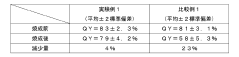
Surface modification techniques are employed to enhance the stability of quantum dots. These include coating quantum dots with protective shells, ligand exchange processes, and surface functionalization with stabilizing agents. Such modifications prevent aggregation, oxidation, and degradation, thereby extending the lifespan and maintaining the optical properties of quantum dots under various environmental conditions.- Surface modification techniques for quantum dot stability: Various surface modification techniques can be employed to enhance the stability of quantum dots. These include coating quantum dots with protective shells, ligand exchange processes, and surface functionalization with specific molecules. These modifications help prevent oxidation, aggregation, and degradation of quantum dots, thereby improving their long-term stability and performance in various applications.
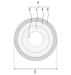
- Core-shell structures for improved quantum dot stability: Core-shell quantum dot structures significantly enhance stability by providing physical barriers against environmental factors. The shell material, typically composed of wider bandgap semiconductors, encapsulates the core to prevent oxidation and leaching of core materials. This architecture also reduces surface defects and passivates dangling bonds, resulting in improved photoluminescence quantum yield and enhanced stability under various operating conditions.
- Polymer encapsulation for quantum dot stabilization: Polymer encapsulation provides an effective method for stabilizing quantum dots against environmental degradation. By embedding quantum dots within polymer matrices or coating them with polymer layers, their resistance to moisture, oxygen, and thermal fluctuations is significantly improved. This approach also enables better dispersion in various media and prevents aggregation, making the quantum dots more suitable for applications in displays, lighting, and biomedical imaging.
- Environmental stability factors for quantum dots: The stability of quantum dots is significantly affected by environmental factors such as temperature, humidity, oxygen exposure, and UV radiation. Research has focused on developing quantum dot compositions and structures that maintain their optical and electronic properties under these challenging conditions. Strategies include the incorporation of stabilizing additives, optimization of synthesis parameters, and development of protective packaging technologies to extend quantum dot lifetime in practical applications.
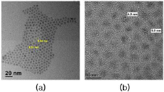
- Manufacturing processes affecting quantum dot stability: The stability of quantum dots is heavily influenced by their manufacturing processes. Precise control over synthesis parameters such as temperature, reaction time, precursor ratios, and purification methods directly impacts the structural integrity and long-term stability of the resulting quantum dots. Advanced manufacturing techniques like microfluidic synthesis, hot-injection methods with controlled cooling, and post-synthesis treatments have been developed to produce quantum dots with enhanced stability characteristics for commercial applications.
02 Core-shell structures for improved stability
Core-shell quantum dot structures significantly improve stability by providing physical barriers against environmental factors. The shell material, typically a semiconductor with a wider bandgap than the core, protects the core from oxidation and chemical degradation while maintaining or enhancing optical properties. Multi-shell structures can further improve stability by providing graded interfaces that reduce lattice strain and surface defects.Expand Specific Solutions03 Encapsulation methods for long-term stability
Encapsulation of quantum dots in matrices such as polymers, silica, or other inorganic materials provides protection from oxygen, moisture, and other environmental factors that cause degradation. These encapsulation methods create physical barriers while maintaining the optical properties of quantum dots, making them suitable for applications requiring long-term stability such as displays, lighting, and biomedical imaging.Expand Specific Solutions04 Stability enhancement through composition control
The stability of quantum dots can be significantly improved through precise control of their composition. This includes alloying the core or shell materials, doping with specific elements, and controlling the stoichiometry of the quantum dot materials. These compositional modifications can reduce defects, improve crystallinity, and enhance resistance to photo-oxidation and thermal degradation.Expand Specific Solutions05 Environmental factors affecting quantum dot stability
Various environmental factors significantly impact quantum dot stability, including temperature, light exposure, pH, and the presence of oxidizing agents. Understanding these factors enables the development of stabilization strategies such as antioxidant additives, UV blockers, and temperature-resistant formulations. These approaches help maintain quantum dot performance in diverse application environments and extend their operational lifetime.Expand Specific Solutions
Key Industry Players in Quantum Nanolithography
Quantum Dot Stability in Advanced Nanolithography is currently in a transitional phase from research to early commercialization, with a global market expected to reach $10.2 billion by 2025. The technology maturity varies significantly across players, with established companies like Samsung Electronics, Nanosys, and 3M leading with robust IP portfolios and commercial applications. Emerging players such as Mojo Vision and QustomDot are advancing specialized applications with innovative approaches to stability challenges. Academic institutions like Xiamen University and University of Toronto contribute fundamental research addressing quantum dot degradation issues. The competitive landscape is characterized by strategic partnerships between materials developers and device manufacturers, with increasing focus on environmentally stable quantum dot formulations for nanolithography applications.
Samsung Electronics Co., Ltd.
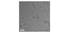
Technical Solution: Samsung Electronics has pioneered advanced quantum dot stabilization techniques specifically optimized for nanolithography applications in semiconductor manufacturing. Their approach combines core-shell nanostructure engineering with surface passivation technologies to create highly stable QDs resistant to degradation during lithographic processes. Samsung's proprietary "QD-Shield" technology employs a gradient alloy interface between core and shell materials, minimizing lattice mismatch and reducing structural defects that typically lead to instability. This technology enables QDs to maintain photoluminescence quantum yields above 85% even after exposure to extreme UV radiation doses typical in advanced lithography. Samsung has also developed specialized silica encapsulation methods that provide hermetic protection while maintaining the QDs' optical properties. Their recent advancements include integration of these stabilized QDs with conventional photoresist materials, creating hybrid systems capable of sub-7nm feature patterning with exceptional edge definition and reduced line-edge roughness compared to traditional lithographic materials.
Strengths: Exceptional stability under extreme UV exposure; seamless integration with existing semiconductor manufacturing infrastructure; superior pattern resolution capabilities. Weaknesses: Complex manufacturing process requiring precise control of multiple parameters; higher initial implementation costs; potential challenges with mass production scalability.
Nanosys, Inc.
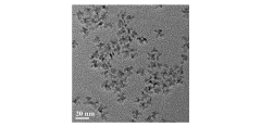
Technical Solution: Nanosys has developed proprietary quantum dot (QD) stabilization technologies for advanced nanolithography applications. Their approach involves encapsulating QDs with specialized ligands and polymer shells that significantly enhance environmental stability while maintaining optical properties. The company's "Hyperion Quantum Dots" technology incorporates a multi-layer protection system that shields QDs from oxygen, moisture, and UV degradation - critical factors in nanolithography processes. Their patented surface modification techniques create strong covalent bonds between the QD core and protective layers, preventing ligand detachment during high-energy lithographic processes. Nanosys has demonstrated QDs with stability at temperatures exceeding 200°C for extended periods, making them suitable for integration with conventional semiconductor manufacturing processes. Their QDs maintain narrow emission linewidths (<30nm FWHM) even after exposure to harsh processing conditions, enabling high-resolution patterning capabilities in the sub-10nm range.
Strengths: Superior thermal stability allowing integration with standard semiconductor processes; exceptional resistance to oxidation and photobleaching; maintains precise optical properties under stress. Weaknesses: Higher production costs compared to conventional materials; potential for batch-to-batch variation affecting lithographic precision; limited compatibility with certain solvents used in lithography.
Critical Patents in Quantum Dot Stabilization
Semiconductor nanomaterial having high stability
PatentActiveJP2022076459A
Innovation
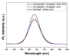
- A quantum dot design with a core composed of InP, a first shell of ZnSe, a second shell, and a graded alloy intermediate layer of In, P, Zn, and Se, which improves lattice alignment and provides a thicker protective shell, maintaining high photoluminescence quantum yield.
Quantum dots capable of improving stability and efficiency and method for manufacturing the same
PatentPendingKR1020240092789A
Innovation
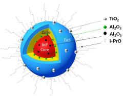
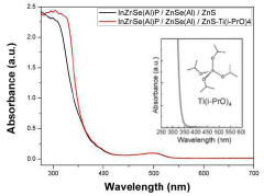
- The quantum dots are manufactured with an InP-based core doped with Al2O3 particles, surrounded by shells of ZnSe, ZnS, and an outermost layer of TiO2, using a method that involves multiple heating steps and the use of isopropoxide ligands to enhance stability and efficiency.
Environmental Impact of Quantum Dot Materials
The environmental impact of quantum dot materials in nanolithography applications represents a significant concern as these technologies advance toward wider commercial deployment. Quantum dots, while offering exceptional optical and electronic properties for high-resolution lithography, contain potentially hazardous elements including cadmium, lead, selenium, and indium that pose substantial environmental and health risks throughout their lifecycle.
Manufacturing processes for quantum dots involve energy-intensive procedures and hazardous chemicals, contributing to considerable carbon footprints and potential environmental contamination. The synthesis typically requires high temperatures, organic solvents, and precursors that generate toxic byproducts requiring specialized disposal protocols. These manufacturing challenges have prompted research into greener synthesis routes using less harmful reagents and lower energy requirements.
Waste management presents another critical environmental consideration. When quantum dot materials reach end-of-life or are discarded during manufacturing, their improper disposal can lead to soil and water contamination. The nanoscale dimensions of these materials enable them to penetrate environmental barriers more readily than conventional pollutants, potentially entering food chains and ecological systems with unpredictable consequences.
Bioaccumulation studies have demonstrated that quantum dots can persist in biological systems, with evidence suggesting potential biomagnification up the food chain. This persistence raises concerns about long-term ecosystem impacts, particularly as the volume of quantum dot materials in circulation increases with broader adoption of advanced nanolithography techniques.
Regulatory frameworks worldwide are evolving to address these environmental concerns. The European Union's Restriction of Hazardous Substances (RoHS) and Registration, Evaluation, Authorization and Restriction of Chemicals (REACH) regulations increasingly scrutinize nanomaterials including quantum dots. Similarly, the United States Environmental Protection Agency has developed specific guidelines for nanomaterial risk assessment and management.
Industry response has focused on developing more environmentally benign alternatives. Recent advances include heavy-metal-free quantum dots using zinc, indium phosphide, or carbon-based structures that maintain optical performance while reducing toxicity. Additionally, closed-loop manufacturing systems are being implemented to capture and recycle quantum dot materials, minimizing environmental release.
Life cycle assessment studies indicate that despite these environmental challenges, quantum dot-based nanolithography may offer net environmental benefits through enabling more energy-efficient electronic devices and more precise manufacturing processes that reduce material waste. However, these benefits must be carefully weighed against the environmental risks throughout the quantum dot lifecycle.
Scalability and Manufacturing Considerations
Scaling quantum dot technology for advanced nanolithography presents significant manufacturing challenges that must be addressed for commercial viability. The transition from laboratory-scale production to industrial-scale manufacturing requires overcoming several critical hurdles. Current quantum dot synthesis methods often suffer from batch-to-batch variations, making consistent quality control difficult when scaling up production volumes. This inconsistency directly impacts the stability and performance of quantum dots in nanolithography applications, where precision at the nanometer scale is essential.
Production yield represents another major consideration, as high-quality quantum dot synthesis typically results in relatively low yields (30-60%) depending on the specific materials and processes used. The manufacturing economics become increasingly challenging when factoring in the expensive precursor materials and specialized equipment required for quantum dot production. These cost factors must be balanced against performance requirements for commercial adoption to be feasible.
Integration with existing semiconductor manufacturing infrastructure presents both opportunities and challenges. While leveraging established fabrication facilities could accelerate adoption, quantum dot processes often require modifications to standard equipment or entirely new process steps. The semiconductor industry's strict requirements for contamination control add another layer of complexity, as quantum dot materials must be processed in ultra-clean environments to prevent impurities that could compromise stability.
Environmental considerations also impact manufacturing scalability. Many traditional quantum dot synthesis methods utilize toxic precursors and solvents that pose health and environmental risks. Developing greener synthesis routes that maintain quantum dot stability while reducing hazardous waste represents an important direction for sustainable manufacturing scale-up. Several research groups have demonstrated promising approaches using microfluidic reactors and continuous flow synthesis to address both environmental concerns and production consistency.
The equipment investment required for large-scale quantum dot manufacturing remains substantial. Specialized reactors capable of precise temperature control, advanced purification systems, and automated quality control instrumentation all contribute to high capital expenditure requirements. Manufacturers must carefully evaluate the return on investment timeline, particularly given the rapidly evolving nature of quantum dot technology and potential for disruptive innovations that could render specific manufacturing approaches obsolete.
Standardization efforts across the industry will be crucial for successful scaling. Currently, the lack of universally accepted standards for quantum dot characterization and performance metrics complicates supplier-customer relationships and technology transfer. Industry consortia and standards organizations have begun addressing this gap, though comprehensive standards remain under development.
Unlock deeper insights with Patsnap Eureka Quick Research — get a full tech report to explore trends and direct your research. Try now!
Generate Your Research Report Instantly with AI Agent
Supercharge your innovation with Patsnap Eureka AI Agent Platform!