Resistive RAM: Emerging Trends and Technical Advances
OCT 9, 20259 MIN READ
Generate Your Research Report Instantly with AI Agent
Patsnap Eureka helps you evaluate technical feasibility & market potential.
ReRAM Technology Background and Objectives
Resistive Random Access Memory (ReRAM) represents a significant advancement in non-volatile memory technology, emerging as a promising alternative to conventional memory solutions. The evolution of ReRAM can be traced back to the early 2000s when researchers began exploring the potential of resistance switching phenomena in various metal oxide materials. This technology leverages the ability to reversibly change the resistance state of a dielectric material, typically a metal oxide, through the application of electrical voltage.
The development trajectory of ReRAM has been characterized by progressive improvements in material science, fabrication techniques, and device architecture. Initially, ReRAM faced challenges related to reliability, endurance, and scalability. However, continuous research efforts have led to substantial enhancements in these areas, positioning ReRAM as a viable candidate for next-generation memory applications.
Current technological trends in ReRAM development focus on optimizing key performance parameters such as switching speed, power consumption, retention time, and endurance cycles. Recent advancements include the exploration of novel materials beyond traditional metal oxides, innovative device structures, and integration strategies with conventional CMOS technology. The trend toward three-dimensional integration and multi-level cell capabilities represents significant steps toward higher density and capacity.
The primary technical objectives for ReRAM development encompass several dimensions. First, achieving higher storage density while maintaining reliability remains a paramount goal. Second, reducing power consumption during both read and write operations is essential for energy-efficient applications. Third, enhancing endurance to support a greater number of write cycles would expand the applicability of ReRAM in various use cases.
Additionally, researchers aim to improve data retention capabilities under diverse environmental conditions, particularly at elevated temperatures. The development of more efficient programming algorithms and error correction techniques represents another critical objective to enhance overall system performance. Integration challenges with existing semiconductor manufacturing processes also constitute a significant focus area.
Looking forward, the ReRAM technology roadmap envisions further miniaturization to sub-10nm nodes, increased multi-level cell capabilities, and enhanced reliability metrics. The ultimate goal is to position ReRAM as a universal memory solution that combines the speed of SRAM, the density of DRAM, and the non-volatility of flash memory, potentially revolutionizing the memory hierarchy in computing systems.
The convergence of these technological advancements and strategic objectives is expected to accelerate the commercial adoption of ReRAM across diverse applications, from Internet of Things (IoT) devices and edge computing to data centers and artificial intelligence systems.
Market Demand Analysis for Non-Volatile Memory
The non-volatile memory (NVM) market is experiencing unprecedented growth driven by the increasing demand for data storage solutions across multiple sectors. Current market analysis indicates that the global NVM market is projected to reach $82 billion by 2025, with a compound annual growth rate (CAGR) of approximately 10.2% from 2020. This growth trajectory is significantly influenced by the expanding applications in consumer electronics, automotive systems, enterprise storage, and emerging IoT devices.
Resistive RAM (ReRAM) represents a particularly promising segment within the broader NVM landscape. While currently occupying a smaller market share compared to established technologies like NAND and NOR flash, ReRAM is gaining traction due to its superior performance characteristics. Market research indicates that ReRAM could capture 15% of the specialty memory market by 2027, representing a substantial opportunity for early adopters and technology developers.
The demand for ReRAM is primarily driven by several key market requirements that traditional memory technologies struggle to address. Power efficiency stands as a critical factor, with data centers and mobile device manufacturers actively seeking solutions that can reduce energy consumption while maintaining performance. ReRAM's low operating voltage and non-volatile nature position it favorably in this regard, potentially reducing memory-related power consumption by up to 40% compared to conventional technologies.
Speed requirements represent another significant market driver. With the proliferation of real-time applications in autonomous vehicles, industrial automation, and edge computing, there is growing demand for memory solutions that can deliver sub-microsecond access times. ReRAM's switching speed advantage over NAND flash makes it particularly attractive for these time-critical applications.
Industry verticals demonstrate varying levels of interest in ReRAM technology. The automotive sector shows particularly strong demand potential, with advanced driver-assistance systems (ADAS) and autonomous driving functions requiring both high reliability and rapid data access. Similarly, the industrial IoT segment values ReRAM's radiation hardness and temperature stability for deployment in harsh environments.
Consumer electronics manufacturers are exploring ReRAM for next-generation mobile devices, where its density advantages could enable greater storage capacity without increasing physical footprint. The enterprise storage market, while more conservative in adoption cycles, recognizes ReRAM's potential for specialized high-performance computing applications where its endurance characteristics provide significant advantages.
Geographic market analysis reveals regional variations in ReRAM demand. Asia-Pacific leads in terms of manufacturing capacity investment, with significant research initiatives in Japan, South Korea, and Taiwan. North America demonstrates strong interest from both technology companies and defense applications, while European markets focus primarily on automotive and industrial implementations.
ReRAM Development Status and Technical Challenges
Resistive RAM (ReRAM) technology has emerged as a promising candidate for next-generation non-volatile memory solutions, offering advantages in scalability, power consumption, and integration capabilities. However, the current development status reveals several significant technical challenges that must be addressed before widespread commercial adoption can be achieved.
The fabrication consistency of ReRAM devices remains a critical issue, with device-to-device and cycle-to-cycle variability presenting major obstacles for mass production. This variability manifests in inconsistent switching voltages, resistance states, and overall performance metrics, making it difficult to guarantee reliable operation across large memory arrays. Statistical analysis of current manufacturing processes indicates variability levels of 15-30% in key performance parameters, which exceeds acceptable thresholds for commercial memory products.
Endurance limitations represent another substantial challenge, with most current ReRAM implementations achieving between 10^6 to 10^9 write cycles before failure. While this exceeds the capabilities of flash memory, it falls short of the requirements for applications such as high-performance computing or enterprise storage systems that demand 10^12 cycles or more. The physical mechanisms behind endurance degradation, including electrode material migration and oxide layer breakdown, require further investigation and mitigation strategies.
Retention characteristics present additional concerns, particularly at elevated temperatures. Current ReRAM technologies demonstrate data retention periods ranging from 5-10 years at room temperature, but this can decrease significantly at higher operating temperatures. The trade-off between fast switching speed and long retention time creates a fundamental design challenge that necessitates novel material systems and device architectures.
The scaling potential of ReRAM faces physical limitations as devices approach sub-10nm dimensions. At these scales, quantum effects and statistical variations in material composition become increasingly pronounced, affecting the stability of the conductive filaments that form the basis of ReRAM operation. Recent research indicates that controlling filament formation and dissolution at these dimensions requires atomic-level precision that exceeds current manufacturing capabilities.
Integration with CMOS technology presents both opportunities and challenges. While ReRAM offers potential for back-end-of-line integration, issues related to thermal budgets, material compatibility, and process contamination must be resolved. Current integration approaches require temperatures below 400°C to maintain CMOS compatibility, limiting material choices and processing options.
The read disturb phenomenon, where repeated reading operations can unintentionally alter stored data, represents a reliability concern that necessitates sophisticated error correction codes and circuit designs. Similarly, write disturb effects can impact adjacent cells in high-density arrays, requiring careful consideration of array architectures and isolation techniques.
Current ReRAM Implementation Approaches
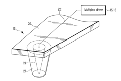
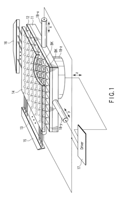
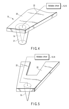
01 Resistive RAM device structures
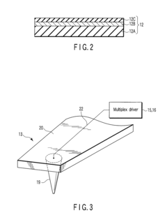
Resistive RAM (RRAM) devices are constructed with specific structures to enable resistive switching behavior. These structures typically include a resistive switching layer sandwiched between two electrodes. Various materials can be used for the resistive switching layer, including metal oxides, chalcogenides, and organic compounds. The electrode materials and their interfaces with the switching layer play crucial roles in determining the device performance. Different structural configurations, such as crossbar arrays, vertical stacks, and 3D architectures, are employed to optimize density, performance, and reliability.- Materials and structures for RRAM devices: Resistive RAM (RRAM) devices utilize specific materials and structures to achieve resistive switching behavior. These typically include metal oxides like HfO2, TiO2, or Ta2O5 as the switching layer sandwiched between electrodes. The structure may incorporate additional layers such as barrier layers or doping elements to enhance performance. The specific arrangement and composition of these materials significantly impact the device's switching characteristics, endurance, and retention properties.
- Switching mechanisms and operation principles: RRAM devices operate based on resistive switching mechanisms where the resistance of the memory cell can be altered between high and low states. This switching behavior is typically attributed to the formation and rupture of conductive filaments within the switching layer, often involving oxygen vacancies or metal ions. The operation principles include SET and RESET processes controlled by applied voltage or current, which modify the internal structure of the switching material to change its resistance state.
- Integration and fabrication techniques: Fabrication of RRAM devices involves specialized techniques to ensure proper integration with existing semiconductor technologies. This includes deposition methods such as atomic layer deposition (ALD), sputtering, or chemical vapor deposition (CVD) for the switching layer, and lithography processes to define device structures. Integration challenges include ensuring compatibility with CMOS processes, minimizing thermal budgets, and developing reliable contact structures to maintain device performance across large arrays.
- Array architecture and addressing schemes: RRAM devices are typically organized in crossbar arrays or other memory architectures to maximize density and performance. These architectures require specific addressing schemes to select individual cells for read and write operations while minimizing interference from neighboring cells. Design considerations include sneak path prevention using selector devices, sense amplifier designs for reliable reading, and peripheral circuitry for efficient programming operations across the memory array.
- Performance enhancement and reliability improvements: Various techniques are employed to enhance RRAM performance and reliability. These include interface engineering to improve switching uniformity, doping strategies to control filament formation, and pulse engineering to optimize programming conditions. Reliability improvements focus on addressing issues such as retention degradation, endurance limitations, and variability between cells. Advanced materials and novel device structures are continuously being developed to overcome these challenges and improve overall device performance.
02 Resistive switching materials and mechanisms
The core functionality of RRAM relies on resistive switching materials that can change their resistance states under applied electric fields. Various mechanisms govern this switching behavior, including filament formation/rupture, interface-type switching, and phase change processes. Metal oxides like HfOx, TaOx, and TiOx are commonly used due to their compatible switching characteristics. The switching mechanism affects key performance parameters such as switching speed, endurance, retention, and power consumption. Understanding and controlling these mechanisms is essential for optimizing RRAM device performance and reliability.Expand Specific Solutions03 RRAM array architecture and integration
RRAM devices are typically organized into memory arrays to achieve high-density storage. Various array architectures are employed, including crossbar arrays, 1T1R (one transistor, one resistor) configurations, and 3D stacking. These architectures address challenges such as sneak path currents, which can cause read disturbances in high-density arrays. Integration with CMOS technology is crucial for practical applications, requiring compatible materials and processes. Peripheral circuits for addressing, sensing, and programming are designed to optimize the overall performance of RRAM memory systems.Expand Specific Solutions04 Programming and operation methods for RRAM
RRAM devices require specific programming methods to reliably switch between resistance states. These methods include voltage pulses with controlled amplitude, duration, and shape to set, reset, and read the memory cells. Various techniques such as compliance current control, multi-level programming, and verify-after-write schemes are employed to improve reliability and enable multi-bit storage. Operating schemes must address challenges like variability, drift, and disturbance effects. Advanced programming algorithms can enhance endurance, retention, and overall reliability of RRAM devices.Expand Specific Solutions05 Applications and specialized RRAM implementations
RRAM technology finds applications beyond conventional memory storage. It is utilized in neuromorphic computing systems to mimic synaptic behavior, enabling efficient implementation of artificial neural networks. RRAM is also employed in security applications like physical unclonable functions (PUFs) and secure memory. Specialized implementations include radiation-hardened RRAM for space applications, ultra-low power RRAM for IoT devices, and high-temperature RRAM for harsh environments. The non-volatile nature and scalability of RRAM make it suitable for various emerging applications in computing and storage systems.Expand Specific Solutions
Key Industry Players in ReRAM Development
Resistive RAM (ReRAM) technology is currently in the early growth phase of its industry lifecycle, transitioning from research to commercialization. The global market is projected to expand significantly, driven by increasing demand for high-density, low-power non-volatile memory solutions. Key players include established semiconductor manufacturers like Samsung Electronics, Micron Technology, SK hynix, and KIOXIA, alongside specialized companies such as CrossBar and Adesto Technologies. Taiwan's semiconductor ecosystem, represented by TSMC, UMC, and Winbond, is making substantial investments in ReRAM development. Research institutions including Fudan University, Peking University, and ITRI are advancing fundamental technologies, while companies like GlobalFoundries and SMIC are working to scale manufacturing processes. The technology's maturity varies across applications, with embedded ReRAM solutions reaching higher readiness levels than standalone memory products.
KIOXIA Corp.
Technical Solution: KIOXIA (formerly Toshiba Memory) has developed a cutting-edge ReRAM technology based on a tantalum oxide switching layer with engineered oxygen vacancy distribution. Their approach utilizes a unique cell structure featuring a tapered filament formation region that enhances switching reliability and reduces cycle-to-cycle variability. KIOXIA's ReRAM demonstrates impressive performance metrics including sub-50ns switching speeds, endurance exceeding 10^6 cycles, and data retention of over 10 years at 85°C[9]. The company has successfully integrated their ReRAM technology with their established semiconductor manufacturing processes at the 40nm node, with ongoing development for more advanced nodes. Their implementation includes proprietary sensing circuits that enable reliable multi-level cell operation, effectively doubling memory density without increasing die size. KIOXIA has demonstrated working prototypes with capacities up to 4Gb, targeting applications in IoT devices, automotive systems, and edge computing where fast, non-volatile memory with low power consumption is critical[10]. Their technology achieves remarkably low read currents (<10μA) while maintaining fast access times.
Strengths: Excellent retention characteristics even at elevated temperatures; low power consumption ideal for battery-powered devices; compatibility with standard CMOS manufacturing processes; potential for cost-effective scaling. Weaknesses: Lower endurance than some competing ReRAM technologies; challenges with resistance drift over extended periods; complex materials engineering requirements; higher manufacturing costs than established memory technologies.
Samsung Electronics Co., Ltd.
Technical Solution: Samsung has pioneered a filamentary ReRAM technology utilizing transition metal oxides (primarily HfO2 and TaOx) as the resistive switching layer. Their approach features a unique dual-layer oxide structure that provides enhanced control over filament formation and dissolution processes. Samsung's ReRAM cells demonstrate remarkable performance with read/write speeds of approximately 10ns, endurance exceeding 10^6 cycles, and data retention of over 10 years at 85°C[3]. The company has successfully integrated their ReRAM technology with their advanced semiconductor manufacturing processes at 28nm node and below. Samsung's implementation includes innovative programming algorithms that mitigate resistance drift issues, enhancing long-term reliability. Their ReRAM architecture incorporates peripheral circuitry designed to minimize read disturb effects and optimize power consumption, achieving operating currents in the microamp range[4]. Samsung has demonstrated working prototypes of high-density ReRAM arrays (multiple Gb) with potential applications in both embedded and standalone memory products.
Strengths: Exceptional scaling potential down to sub-10nm nodes; compatibility with Samsung's established manufacturing infrastructure; low power consumption compared to flash memory; potential for 3D stacking to achieve higher densities. Weaknesses: Resistance variability between cycles affecting reliability; requires complex materials engineering; higher production costs than conventional memory technologies; thermal stability challenges at elevated operating temperatures.
Critical Patents and Technical Innovations in ReRAM
Resistive ram and fabrication method
PatentActiveUS20140264237A1
Innovation
- The method involves forming a nitrogen-containing metal oxide layer, such as tungsten oxynitride, over a transition metal electrode using a rapid thermal oxidation process, which reduces the forming voltage and improves the flatness of the metal oxide surface, facilitating subsequent processing and enhancing device performance by lowering the set and reset voltages.
Information recording/reproducing device having head covering by resistance element
PatentInactiveUS8050171B2
Innovation
- Incorporating a resistance element on the conductive region of the probe head for reading servo burst signals, allowing for smooth intensity changes based on position deviation, enabling precise position control and high sensitivity data reproduction.
Materials Science Advancements for ReRAM
Material science innovations represent the cornerstone of ReRAM advancement, with significant progress in both oxide and non-oxide based materials. Metal oxides such as HfOx, TaOx, and TiOx have emerged as leading candidates due to their excellent switching characteristics, compatibility with CMOS processes, and thermal stability. These materials demonstrate reliable resistive switching behavior with high ON/OFF ratios exceeding 10^6 in some cases, while maintaining data retention periods of over 10 years at operating temperatures.
Recent breakthroughs in two-dimensional (2D) materials have opened new frontiers for ReRAM development. Transition metal dichalcogenides (TMDs) like MoS2 and WSe2 exhibit unique electronic properties that enable ultra-thin switching layers, potentially reducing power consumption by up to 70% compared to conventional oxide-based devices. These materials demonstrate exceptional mechanical flexibility, making them particularly suitable for next-generation flexible and wearable electronics applications.
Polymer-based ReRAM represents another promising direction, with materials such as PMMA (polymethyl methacrylate) and PVA (polyvinyl alcohol) showing tunable resistance states through conformational changes in polymer chains. These organic materials offer advantages in solution processability, mechanical flexibility, and biocompatibility, though they currently lag behind inorganic counterparts in switching speed and endurance.
Interface engineering has become a critical focus area, with researchers developing sophisticated multi-layer structures to control ion migration pathways. The introduction of engineered defects and dopants at material interfaces has demonstrated improved switching uniformity and reduced cycle-to-cycle variability. For instance, oxygen vacancy engineering in HfOx-based devices has shown to reduce the standard deviation in set/reset voltages by nearly 40%.
Atomic layer deposition (ALD) and pulsed laser deposition (PLD) techniques have revolutionized the fabrication of high-quality, ultra-thin films with precise thickness control down to sub-nanometer levels. These advanced deposition methods enable the creation of complex heterostructures with atomically sharp interfaces, critical for reliable ReRAM operation.
The integration of novel electrode materials, including graphene, carbon nanotubes, and metallic nitrides, has addressed issues related to electrode degradation and metal diffusion. These materials provide enhanced stability during repeated switching cycles while maintaining low contact resistance, extending device lifetime by orders of magnitude compared to conventional metal electrodes.
Energy Efficiency and Scaling Considerations
Energy efficiency represents a critical factor in the advancement and commercial viability of Resistive RAM (RRAM) technology. Current RRAM devices demonstrate significant advantages over conventional memory technologies, with power consumption during write operations typically ranging from 10 to 100 times lower than flash memory. This remarkable efficiency stems from RRAM's fundamental operating principle, which requires minimal energy to form and disrupt conductive filaments within the resistive switching material.
The scaling potential of RRAM further enhances its energy profile. As device dimensions decrease to sub-20nm nodes, RRAM maintains functional integrity while achieving proportionally lower power consumption. Recent research demonstrates successful operation of RRAM cells at dimensions below 10nm, with corresponding reduction in programming currents to the microampere or even nanoampere range. This scaling advantage positions RRAM as an exceptionally promising candidate for ultra-low-power applications in IoT devices, edge computing, and mobile systems.
Thermal efficiency considerations also play a crucial role in RRAM development. Unlike phase-change memory (PCM), which requires substantial thermal energy for state transitions, RRAM's filamentary switching mechanism operates primarily through electric field effects, minimizing heat generation. This characteristic enables higher cell density without thermal crosstalk concerns and reduces cooling requirements in high-density memory arrays.
Innovative material engineering approaches have further enhanced RRAM's energy profile. Multi-layer oxide structures, doped switching materials, and engineered interfaces have demonstrated programming voltages below 1V while maintaining reliable retention characteristics. These advancements address the historical challenge of balancing low-power operation with data stability, particularly in embedded applications where power constraints are stringent.
The read operation efficiency of RRAM also merits attention. With resistance ratios (ROFF/RON) exceeding 103 in advanced devices, read operations can be performed at extremely low voltages (typically 0.1-0.3V), minimizing read disturb phenomena while ensuring accurate state detection. This characteristic proves especially valuable in neuromorphic computing applications, where frequent read operations dominate energy consumption profiles.
Looking forward, emerging research in quantum-assisted switching mechanisms and two-dimensional material-based RRAM promises to push energy efficiency boundaries even further. Theoretical models suggest potential operation at the thermodynamic limit, approaching femtojoule-per-bit energy consumption—a paradigm shift that could revolutionize the memory hierarchy in next-generation computing systems.
Unlock deeper insights with Patsnap Eureka Quick Research — get a full tech report to explore trends and direct your research. Try now!
Generate Your Research Report Instantly with AI Agent
Supercharge your innovation with Patsnap Eureka AI Agent Platform!