Resistive RAM: Market Forces and Industry Movements
OCT 9, 20259 MIN READ
Generate Your Research Report Instantly with AI Agent
Patsnap Eureka helps you evaluate technical feasibility & market potential.
ReRAM Technology Background and Objectives
Resistive Random Access Memory (ReRAM) has emerged as a promising non-volatile memory technology over the past two decades, evolving from fundamental research in the early 2000s to commercial product development in recent years. The technology leverages the resistance switching phenomenon in certain metal oxide materials, where electrical resistance can be altered through the application of voltage, creating stable states that represent binary data. This resistance change mechanism offers significant advantages over traditional memory technologies, including lower power consumption, faster switching speeds, and enhanced durability.
The evolution of ReRAM technology has been driven by the increasing limitations of conventional memory solutions such as DRAM and NAND flash. As semiconductor scaling approaches physical limits, traditional memory technologies face challenges in maintaining performance improvements while managing power consumption. ReRAM presents a potential solution to these challenges, positioning itself as a bridge between the speed of SRAM and the non-volatility of flash memory.
Industry trends indicate a growing interest in ReRAM as part of the broader emerging non-volatile memory landscape. The technology has progressed through several generations, with early implementations focusing on binary metal oxide structures, while more recent developments explore complex multi-layer architectures and novel materials to enhance performance characteristics. Research milestones include the demonstration of sub-10nm ReRAM cells, multi-level cell capabilities, and integration with conventional CMOS processes.
The primary technical objectives for ReRAM development center around addressing key performance parameters that will enable broader market adoption. These include improving write endurance beyond 10^9 cycles, reducing switching energy to compete with established technologies, enhancing data retention at elevated temperatures, and developing reliable manufacturing processes that maintain consistent performance across billions of memory cells.
Current research is particularly focused on understanding and controlling the filament formation mechanisms that underlie ReRAM operation. This fundamental knowledge is critical for optimizing device characteristics and ensuring reliable performance across various operating conditions. Material innovation represents another significant research direction, with exploration of new switching materials and electrode combinations to enhance switching characteristics.
The technology roadmap for ReRAM envisions progression from current niche applications in IoT and embedded systems toward more mainstream memory markets. Near-term objectives include perfecting embedded ReRAM solutions for microcontrollers and specialized applications, while medium-term goals target standalone memory products that could potentially replace certain segments of the flash memory market.
Long-term strategic objectives for ReRAM technology include achieving the density and cost metrics necessary to compete in mass storage applications, while maintaining its inherent advantages in speed and power efficiency. The ultimate vision positions ReRAM as a universal memory technology that could potentially bridge the traditional memory hierarchy, offering both storage and working memory capabilities in a single technology platform.
Market Demand Analysis for Non-Volatile Memory
The non-volatile memory market has experienced significant growth in recent years, driven by increasing demand for data storage solutions across various industries. The global non-volatile memory market was valued at approximately $67 billion in 2021 and is projected to reach $125 billion by 2028, growing at a CAGR of around 9.3% during the forecast period. This growth is primarily fueled by the expanding applications in consumer electronics, automotive systems, enterprise storage, and emerging technologies like IoT and AI.
Resistive RAM (ReRAM) represents a promising segment within the non-volatile memory landscape, positioned to address limitations of existing technologies. While NAND flash currently dominates the market with over 70% share, its scaling challenges and performance limitations are creating opportunities for next-generation alternatives like ReRAM. Industry analysts predict ReRAM could capture up to 15% of the non-volatile memory market by 2030, representing a potential market value exceeding $20 billion.
The demand for ReRAM is particularly strong in applications requiring high endurance, low power consumption, and fast switching speeds. The automotive sector, expected to grow at 12% CAGR through 2028, represents a significant opportunity as advanced driver-assistance systems and autonomous vehicles require reliable, high-performance memory solutions capable of operating in extreme conditions. Similarly, the industrial IoT segment, growing at 11% annually, demands memory technologies with extended lifecycle and minimal maintenance requirements.
Enterprise storage systems are increasingly adopting non-volatile memory solutions to address the growing data processing requirements. With data centers worldwide managing over 175 zettabytes of data by 2025, the need for energy-efficient, high-density storage solutions becomes critical. ReRAM's potential for 3D stacking and multi-level cell architectures positions it favorably in this high-growth segment.
Consumer electronics continues to be the largest application segment for non-volatile memory, accounting for approximately 45% of the market. The trend toward edge computing in smartphones, wearables, and smart home devices is creating demand for memory solutions that combine the speed of DRAM with the non-volatility of flash, a niche where ReRAM shows particular promise.
Geographically, Asia-Pacific represents the largest market for non-volatile memory technologies, accounting for over 60% of global consumption, driven by the concentration of semiconductor manufacturing and consumer electronics production. North America follows with approximately 20% market share, with particularly strong demand in enterprise storage and data center applications where ReRAM's performance advantages are most valuable.
The market demand for ReRAM is further bolstered by increasing requirements for radiation-hardened memory in aerospace and defense applications, a specialized segment growing at 7% annually and valuing reliability and performance over cost considerations.
ReRAM Technical Challenges and Global Development Status
ReRAM technology faces several significant technical challenges despite its promising potential. One of the primary obstacles is the variability in resistance states, which affects data reliability and retention. This inconsistency stems from the stochastic nature of filament formation and rupture processes within the memory cells, creating unpredictable switching behaviors that complicate large-scale implementation.
Endurance limitations represent another critical challenge, with current ReRAM devices typically achieving 10^6 to 10^9 write cycles—significantly lower than the industry standard for DRAM. This limitation restricts ReRAM's application in write-intensive scenarios and necessitates sophisticated wear-leveling algorithms to extend device lifespan.
The sneak path current problem in crossbar array architectures continues to impede high-density integration. Although selector devices and complementary resistive switching mechanisms have been proposed as solutions, they introduce additional complexity and manufacturing challenges that impact yield rates and production costs.
Globally, ReRAM development exhibits distinct regional characteristics. The United States leads in fundamental research and intellectual property, with companies like Crossbar, Weebit Nano, and Intel making significant advancements. These organizations focus on developing proprietary materials and architectures to overcome the aforementioned technical barriers.
Asian markets, particularly Japan, South Korea, and Taiwan, demonstrate strength in manufacturing infrastructure and integration capabilities. Companies such as Panasonic, Samsung, and TSMC have made substantial investments in pilot production lines, focusing on process optimization and yield improvement for commercial viability.
European research institutions contribute significantly to materials science innovations and alternative ReRAM structures. Their collaborative approach with industry partners has yielded novel solutions for reliability and endurance issues, though commercialization lags behind other regions.
China has rapidly accelerated its ReRAM development efforts through national semiconductor initiatives, with emerging players like YMTC and research partnerships between universities and state-backed enterprises focusing on indigenous technology development to reduce dependency on foreign intellectual property.
The scaling challenge remains universal across all regions, as reducing cell dimensions below 10nm introduces quantum effects that alter resistive switching mechanisms. This fundamental physical limitation requires innovative materials engineering and device architectures to maintain reliable performance at advanced technology nodes.
Current ReRAM Implementation Solutions
01 Materials and structures for RRAM devices
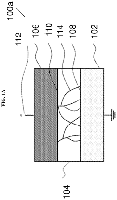
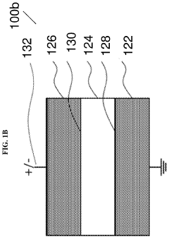
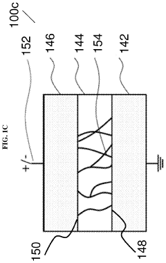
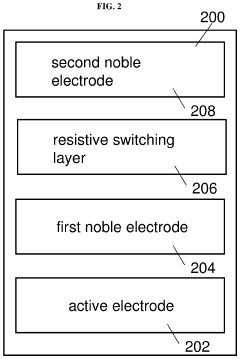
Resistive Random Access Memory (RRAM) devices utilize specific materials and structures to enable resistive switching behavior. These typically include metal oxides like HfO2, TiO2, or Ta2O5 as the switching layer sandwiched between two electrodes. The structure may incorporate additional layers such as barrier layers or doping elements to enhance performance. The specific arrangement and composition of these materials significantly impact the device's switching characteristics, endurance, and retention properties.- Resistive RAM device structures: Resistive RAM (RRAM) devices are constructed with specific structural configurations to optimize performance. These structures typically include a resistive switching layer sandwiched between two electrodes. Various materials can be used for the resistive layer, including metal oxides, chalcogenides, and perovskites. The electrode materials and their interfaces with the resistive layer play crucial roles in determining switching characteristics. Advanced structures may incorporate additional layers for improved stability, retention, and endurance.
- Resistive switching mechanisms: The operation of resistive RAM relies on various switching mechanisms that enable transitions between high and low resistance states. These mechanisms include filamentary conduction, where conductive filaments form and rupture within the resistive layer, and interface-type switching, where resistance changes occur at electrode-oxide interfaces. Other mechanisms involve oxygen vacancy migration, ion migration, or phase changes in the switching material. Understanding these mechanisms is essential for designing RRAM devices with improved reliability, endurance, and switching speed.
- Integration and fabrication techniques: Fabrication of resistive RAM involves specialized techniques to ensure device performance and compatibility with existing semiconductor processes. These include deposition methods like atomic layer deposition, sputtering, and chemical vapor deposition for creating uniform resistive layers. Integration challenges include ensuring CMOS compatibility, managing thermal budgets, and developing 3D stacking approaches. Advanced patterning techniques and materials engineering are employed to achieve high-density memory arrays while maintaining reliable switching characteristics.
- Circuit design and operation: Circuit designs for resistive RAM systems address unique operational requirements including programming, reading, and erasing operations. These circuits manage the application of voltage pulses with specific amplitudes and durations to control resistance switching. Sensing circuits detect the resistance state with high accuracy while minimizing read disturbance. Advanced designs incorporate features for multi-level cell operation, error correction, and wear-leveling to extend device lifetime. Power management circuits optimize energy consumption during both active and standby modes.
- Novel materials for resistive switching: Research on novel materials aims to enhance resistive RAM performance metrics including retention, endurance, and switching speed. Materials under investigation include complex metal oxides, two-dimensional materials, and organic compounds. Doping strategies and interface engineering are employed to control defect concentrations and migration barriers. Nanocomposite materials combine the advantages of different material systems to achieve optimized switching characteristics. These material innovations address challenges related to variability, reliability, and scalability of resistive memory devices.
02 Switching mechanisms and operation principles
RRAM devices operate based on the formation and rupture of conductive filaments within an insulating layer, causing resistance changes between high and low resistance states. The switching mechanism typically involves oxygen vacancy migration, metal ion movement, or phase changes in the switching material. These devices can be operated in unipolar or bipolar switching modes, with different voltage polarities controlling the set and reset processes. Understanding these mechanisms is crucial for optimizing device performance and reliability.Expand Specific Solutions03 Integration and fabrication techniques
Fabrication of RRAM devices involves specialized techniques to ensure proper formation of the resistive switching layer and electrode interfaces. These include atomic layer deposition, physical vapor deposition, and various etching processes. Integration challenges include compatibility with CMOS processes, 3D stacking capabilities, and scaling to smaller technology nodes. Advanced fabrication methods focus on controlling film thickness, interface quality, and defect concentration to achieve consistent switching behavior and improved device yield.Expand Specific Solutions04 Performance enhancement and reliability
Improving RRAM performance involves addressing key challenges such as endurance, retention, and variability. Techniques include interface engineering, doping of the switching layer, and optimizing programming conditions. Reliability enhancement methods focus on controlling filament formation, preventing over-programming, and mitigating degradation mechanisms. Advanced architectures may incorporate selector devices to minimize sneak path currents in crossbar arrays or employ multi-level cell approaches to increase storage density.Expand Specific Solutions05 Circuit design and memory applications
RRAM implementation in memory systems requires specialized circuit designs for read, write, and erase operations. These include sense amplifiers, programming drivers, and address decoders optimized for resistive switching characteristics. RRAM can be configured in various array architectures such as crossbar arrays or 1T1R (one transistor, one resistor) structures. Beyond conventional memory applications, RRAM shows promise for neuromorphic computing, in-memory computing, and security applications due to its analog switching behavior and non-volatile characteristics.Expand Specific Solutions
Key Industry Players and Competitive Landscape
The Resistive RAM (ReRAM) market is currently in a growth phase, transitioning from research to commercialization with an estimated market size of $1.2-1.5 billion, expected to expand significantly as IoT and AI applications increase demand for efficient memory solutions. The technology maturity varies across players, with established semiconductor giants like Samsung, Micron, Intel, and TSMC investing heavily in R&D while specialized companies like Adesto, Everspin, and Innostar Semiconductor are developing commercial ReRAM products. Academic-industry partnerships are accelerating development, with institutions like Peking University and National University of Singapore collaborating with companies to overcome technical challenges in scalability, endurance, and retention. Asian manufacturers, particularly KIOXIA, Macronix, and Winbond, are emerging as key players in the ReRAM ecosystem.
KIOXIA Corp.
Technical Solution: KIOXIA (formerly Toshiba Memory) has developed an innovative Resistive RAM technology based on their proprietary filament-type switching mechanism. Their approach utilizes transition metal oxides in a vertical ReRAM (VReRAM) architecture that enables high-density storage with improved reliability. KIOXIA's ReRAM technology features switching speeds under 50ns, endurance of approximately 10^6 cycles, and excellent data retention characteristics at elevated temperatures. The company has focused on integrating their ReRAM technology into embedded systems for IoT applications, automotive electronics, and industrial control systems where power efficiency and non-volatility are critical. KIOXIA has also explored using ReRAM as a storage class memory (SCM) solution that bridges the performance gap between DRAM and NAND flash in data center applications.
Strengths: Strong background in memory technology development, established manufacturing infrastructure, and expertise in reliability engineering. KIOXIA's ReRAM shows excellent retention characteristics at high temperatures. Weaknesses: Challenges in achieving consistent switching behavior across large arrays, and competition from alternative emerging memory technologies.
Micron Technology, Inc.
Technical Solution: Micron has developed a proprietary Resistive RAM technology called 3D XPoint (developed jointly with Intel before becoming solely Micron's project). Their approach uses chalcogenide materials in a crosspoint architecture that enables non-volatile memory with performance characteristics between DRAM and NAND flash. Micron's ReRAM technology demonstrates read latencies of approximately 100ns, write latencies of about 500ns, and endurance ratings of 10^7-10^9 cycles. The company has focused on optimizing their ReRAM for data center applications, particularly for AI workloads and real-time analytics that require high-speed, non-volatile memory solutions. Micron has also explored hybrid memory systems that combine ReRAM with conventional memory technologies to create tiered storage solutions that optimize both performance and cost.
Strengths: Extensive memory manufacturing expertise, established market presence, and strong IP portfolio in memory technologies. Micron's ReRAM offers superior endurance compared to NAND flash. Weaknesses: Higher cost per bit compared to conventional storage solutions, and challenges in achieving mass production yields comparable to mature memory technologies.
Critical Patents and Technical Innovations in ReRAM
Memory cell and method of forming the same
PatentActiveUS20210013407A1
Innovation
- A memory cell design featuring a hybrid noble-active electrode structure with a patterned noble electrode and a continuous active electrode, along with a resistive switching layer, is proposed. This structure confines conduction paths within well-defined regions, enhancing switching uniformity and reducing power consumption by up to 40 times.
Information recording/reproducing device having head covering by resistance element
PatentInactiveUS8050171B2
Innovation
- Incorporating a resistance element on the conductive region of the probe head for reading servo burst signals, allowing for smooth intensity changes based on position deviation, enabling precise position control and high sensitivity data reproduction.
Supply Chain Analysis for ReRAM Manufacturing
The ReRAM manufacturing supply chain represents a complex ecosystem involving multiple stakeholders across various geographical regions. Raw material suppliers constitute the foundation of this chain, providing essential components such as transition metal oxides (including HfO2, TiO2, and Ta2O5), electrode materials (platinum, titanium nitride, tungsten), and silicon substrates. These materials predominantly originate from regions with established mining and refining capabilities, including China, Japan, South Korea, and the United States.
Fabrication equipment manufacturers form another critical link, supplying specialized tools for atomic layer deposition (ALD), physical vapor deposition (PVD), and etching processes. Companies like Applied Materials, Lam Research, and Tokyo Electron dominate this segment, with their manufacturing bases concentrated in the United States, Japan, and Europe.
The actual ReRAM device fabrication occurs primarily in semiconductor foundries, with Taiwan Semiconductor Manufacturing Company (TSMC), Samsung, and SK Hynix leading production capabilities. These foundries have established specialized process flows for ReRAM integration, either as standalone memory or embedded within logic circuits. The geographical concentration of these facilities in East Asia creates potential supply chain vulnerabilities.
Testing and packaging operations represent downstream activities, with specialized equipment providers like Advantest and Teradyne supplying memory testing solutions. These operations are distributed across Taiwan, China, Malaysia, and the Philippines, creating a geographically diverse but logistically complex final production stage.
Current supply chain challenges include material consistency issues, particularly in oxide layer composition control, which directly impacts device reliability and endurance. Additionally, the industry faces equipment compatibility challenges when integrating ReRAM processes into existing semiconductor manufacturing lines, often requiring specialized modifications to standard tools.
The ReRAM supply chain also exhibits significant concentration risk, with over 70% of advanced manufacturing capacity located in East Asia. This geographical concentration creates vulnerability to regional disruptions, as evidenced during recent global semiconductor shortages. Furthermore, intellectual property fragmentation across multiple players complicates technology transfer and standardization efforts.
Future supply chain optimization opportunities include vertical integration strategies being pursued by major memory manufacturers, development of specialized ReRAM-specific fabrication equipment, and emerging partnerships between material suppliers and device manufacturers to improve material consistency and performance characteristics.
Energy Efficiency and Sustainability Aspects of ReRAM
Energy efficiency has emerged as a critical factor in the adoption and development of Resistive RAM (ReRAM) technologies. ReRAM demonstrates significant advantages in power consumption compared to conventional memory technologies, with studies indicating up to 10-100x lower operational energy requirements than NAND flash memory. This efficiency stems from ReRAM's fundamental operating principle, which eliminates the need for constant refresh cycles present in DRAM and reduces the high programming voltages required by flash memory.
The standby power consumption of ReRAM is particularly noteworthy, with leakage currents orders of magnitude lower than competing technologies. This characteristic makes ReRAM especially suitable for edge computing devices and IoT applications where battery life and thermal management are paramount concerns. Recent advancements in material science have further reduced the switching energy of ReRAM cells to sub-pJ levels, representing a significant milestone in memory technology efficiency.
From a sustainability perspective, ReRAM offers several environmental advantages throughout its lifecycle. The manufacturing process for ReRAM typically requires fewer processing steps than traditional memory technologies, potentially reducing resource consumption and waste generation. Additionally, many ReRAM designs utilize abundant materials like silicon oxide and titanium oxide, avoiding the dependency on rare or environmentally problematic elements found in some other emerging memory technologies.
The extended endurance capabilities of ReRAM—with some implementations demonstrating 10^12 write cycles—contribute to sustainability by extending device lifespans and reducing electronic waste. This longevity factor is increasingly important as embedded memory becomes more prevalent in consumer electronics and industrial systems where replacement cycles impact environmental footprints.
Industry leaders have recognized these sustainability benefits, with companies like Weebit Nano and Crossbar highlighting the green technology aspects of their ReRAM solutions. Market analysis indicates that energy efficiency has become a primary driver for ReRAM adoption in data centers, where memory operations can account for 25-40% of total power consumption. The potential energy savings at scale represent both economic and environmental value propositions that are reshaping investment priorities in memory technology development.
Looking forward, research trends suggest further improvements in ReRAM energy profiles through innovations in selector devices, interface engineering, and advanced materials. These developments align with global initiatives for green computing and sustainable electronics, positioning ReRAM as a key technology in the broader movement toward environmentally responsible digital infrastructure.
Unlock deeper insights with Patsnap Eureka Quick Research — get a full tech report to explore trends and direct your research. Try now!
Generate Your Research Report Instantly with AI Agent
Supercharge your innovation with Patsnap Eureka AI Agent Platform!