

Resistive RAM Performance: A Comparative Analysis of Materials
OCT 9, 202510 MIN READ
Generate Your Research Report Instantly with AI Agent
PatSnap Eureka helps you evaluate technical feasibility & market potential.
ReRAM Technology Background and Objectives
Resistive Random Access Memory (ReRAM) has emerged as a promising candidate for next-generation non-volatile memory technologies, offering potential advantages in terms of power consumption, scalability, and integration capabilities. The evolution of ReRAM technology can be traced back to the early 2000s when researchers began exploring the resistive switching phenomena in various metal oxide materials. Since then, significant advancements have been made in understanding the underlying mechanisms and improving device performance.
The technological trajectory of ReRAM has been characterized by continuous improvements in switching speed, endurance, retention time, and power efficiency. Early ReRAM devices suffered from reliability issues, including inconsistent switching behavior and limited endurance. However, recent developments have addressed many of these challenges through materials engineering and device architecture optimization, leading to more stable and reliable devices.
Material selection has proven to be a critical factor in determining ReRAM performance characteristics. Various materials including metal oxides (HfOx, TaOx, TiOx), chalcogenides, and perovskites have demonstrated resistive switching behavior, each offering distinct advantages and limitations. The diversity of materials has enabled the customization of ReRAM devices for specific applications, ranging from high-density storage to neuromorphic computing.
The primary technical objectives for ReRAM development include achieving higher density integration, reducing operating voltage and power consumption, enhancing endurance beyond 10^12 cycles, extending retention time to over 10 years, and improving switching speed to sub-nanosecond levels. Additionally, there is a growing emphasis on developing multi-level cell capabilities to increase storage density and exploring novel applications beyond conventional memory.
Industry trends indicate a shift towards heterogeneous integration, where ReRAM is combined with conventional CMOS technology to create hybrid memory solutions. This approach leverages the strengths of both technologies while mitigating their respective limitations. Furthermore, the compatibility of ReRAM with back-end-of-line (BEOL) processes makes it particularly attractive for 3D integration, potentially enabling unprecedented memory densities.
The comparative analysis of different materials for ReRAM applications reveals a complex landscape where performance metrics often involve trade-offs. For instance, HfOx-based devices typically offer excellent endurance but may require higher operating voltages, while TaOx-based devices can operate at lower voltages but might exhibit more variability in switching behavior. Understanding these material-dependent characteristics is essential for optimizing ReRAM technology for specific use cases.
Looking forward, the ReRAM technology roadmap aims to address remaining challenges related to device variability, reliability at scaled dimensions, and integration with existing memory hierarchies. The ultimate goal is to position ReRAM as a versatile memory solution capable of bridging the performance gap between high-speed volatile memories and high-density storage technologies.
Market Analysis for ReRAM Applications
The global ReRAM (Resistive Random Access Memory) market is experiencing significant growth, with projections indicating an expansion from $1.2 billion in 2023 to approximately $4.6 billion by 2028, representing a compound annual growth rate (CAGR) of 30.8%. This remarkable growth trajectory is primarily driven by increasing demand for high-performance, energy-efficient memory solutions across multiple sectors.
The consumer electronics segment currently dominates the ReRAM market, accounting for approximately 42% of total market share. This dominance stems from the growing integration of ReRAM in smartphones, tablets, and wearable devices, where its low power consumption and high-speed operation provide significant advantages over traditional memory technologies.
Enterprise storage systems represent the second-largest application segment, with approximately 28% market share. The ability of ReRAM to offer non-volatile storage with DRAM-like performance makes it particularly attractive for data centers seeking to reduce energy consumption while maintaining high-speed data access capabilities.
Automotive applications are emerging as the fastest-growing segment, with a projected CAGR of 36.5% through 2028. Advanced driver-assistance systems (ADAS) and autonomous vehicles require memory solutions that can withstand extreme temperatures and offer radiation hardness – characteristics inherent to certain ReRAM material compositions, particularly those utilizing hafnium oxide and tantalum oxide.
Industrial IoT applications are also driving significant demand, with the segment expected to grow at a CAGR of 33.7%. ReRAM's combination of low power consumption, high endurance, and radiation resistance makes it ideal for remote sensing applications and industrial control systems operating in harsh environments.
Geographically, North America currently leads the market with approximately 38% share, followed by Asia-Pacific at 35% and Europe at 22%. However, the Asia-Pacific region is expected to witness the highest growth rate, driven by increasing semiconductor manufacturing capabilities and rising electronic device production in countries like China, South Korea, and Taiwan.
Material selection significantly impacts market adoption across these segments. Hafnium oxide-based ReRAM dominates with approximately 45% market share due to its CMOS compatibility and reliability. Tantalum oxide compositions follow at 30%, while perovskite-based solutions are gaining traction in specialized applications requiring extreme temperature tolerance.
The market faces challenges including manufacturing scalability issues and competition from emerging memory technologies like MRAM and FeRAM. However, recent advancements in material engineering and fabrication processes are gradually addressing these limitations, positioning ReRAM for accelerated market penetration across diverse application domains.
Current ReRAM Material Challenges
Despite significant advancements in ReRAM technology, several material-related challenges continue to impede its widespread commercial adoption. The primary challenge remains the trade-off between retention and switching speed, which is fundamentally tied to the materials used in the switching layer. Metal oxides like HfOx and TaOx demonstrate excellent retention characteristics but suffer from slower switching speeds, while materials with faster switching often exhibit poor data retention properties.
Variability in switching behavior represents another critical challenge, manifesting as cycle-to-cycle and device-to-device variations. This inconsistency stems from the stochastic nature of filament formation and rupture processes, which are heavily influenced by material composition, defect distribution, and interface properties. Materials with more uniform microstructures and controlled defect concentrations are being investigated to address this issue.
Endurance limitations present a significant barrier to ReRAM implementation in applications requiring frequent write operations. Current materials typically achieve 10^6 to 10^9 switching cycles before failure, falling short of the 10^15 cycles demonstrated by conventional SRAM. Material degradation mechanisms include electrode metal diffusion, oxygen vacancy clustering, and interface layer deterioration, all of which contribute to eventual device failure.
Power consumption during SET and RESET operations remains higher than ideal for many low-power applications. The current densities required for reliable filament formation and dissolution directly correlate with the energetic barriers determined by material properties. Researchers are exploring materials with lower formation energies for oxygen vacancies and optimized electrode-oxide interfaces to reduce operational voltages.
Scaling challenges become increasingly prominent as device dimensions shrink below 10nm. At these scales, material properties can deviate significantly from bulk behavior, and filament formation becomes less predictable. Quantum confinement effects and increased surface-to-volume ratios alter electronic properties, requiring novel material engineering approaches to maintain reliable operation at advanced technology nodes.
Temperature stability represents another material challenge, with many ReRAM materials showing significant performance degradation outside narrow temperature ranges. This limitation restricts their application in automotive, industrial, and aerospace environments where wide temperature operation is essential. Materials with more robust temperature coefficients and thermally stable interfaces are being investigated to address this limitation.
Manufacturing integration challenges also persist, particularly regarding compatibility with CMOS processes. Many promising ReRAM materials require processing conditions that can damage existing CMOS layers or introduce contamination. Finding materials that maintain their switching properties while being compatible with standard semiconductor fabrication flows remains an ongoing challenge for the industry.
Material Solutions for ReRAM Performance
01 Materials and structures for improved RRAM performance
Various materials and structural designs can enhance resistive RAM performance. These include using specific metal oxides, doped materials, and engineered interfaces between layers. Multi-layer structures with carefully selected materials can improve switching characteristics, retention, and endurance. The arrangement of electrodes and the composition of the switching layer significantly impact the overall performance of RRAM devices.- Material composition for improved RRAM performance: The performance of resistive RAM can be significantly enhanced through the optimization of material composition. Various materials such as metal oxides, chalcogenides, and perovskites are used as the switching layer in RRAM devices. The selection and engineering of these materials directly impact key performance metrics including switching speed, endurance, and retention time. Doping strategies and interface engineering between the electrode and switching layer can further improve the stability and reliability of RRAM devices.
- Device structure optimization for RRAM: The structural design of resistive RAM devices plays a crucial role in determining their performance characteristics. Various architectural approaches such as crossbar arrays, 3D stacking, and multi-layer configurations can be implemented to enhance density, reduce power consumption, and improve operational stability. The geometry and dimensions of the memory cell, including the thickness of the switching layer and electrode configuration, significantly impact the forming voltage, SET/RESET operations, and overall reliability of the RRAM device.
- Switching mechanisms and operational parameters: Understanding and controlling the switching mechanisms in resistive RAM is essential for optimizing performance. The formation and rupture of conductive filaments, ion migration, and interface effects contribute to the resistive switching behavior. Operational parameters such as compliance current, pulse width, and voltage amplitude significantly affect the switching characteristics, including the ON/OFF ratio, switching speed, and energy consumption. Advanced control schemes can be implemented to achieve more reliable and efficient switching operations.
- Integration and fabrication techniques: Advanced fabrication and integration techniques are crucial for realizing high-performance resistive RAM devices. Process optimization including deposition methods, annealing conditions, and patterning techniques directly impact device uniformity and yield. CMOS compatibility is essential for enabling the integration of RRAM with conventional semiconductor technology. Novel approaches such as atomic layer deposition and self-assembly techniques can be employed to achieve precise control over the material interfaces and structural features, resulting in improved device performance and reliability.
- Testing and reliability enhancement methods: Comprehensive testing methodologies and reliability enhancement techniques are essential for evaluating and improving RRAM performance. Accelerated lifetime testing, cycling endurance tests, and data retention measurements provide insights into the long-term stability of RRAM devices. Various techniques such as error correction codes, adaptive programming schemes, and wear-leveling algorithms can be implemented to enhance reliability and extend device lifetime. Advanced characterization methods including in-situ TEM and conductive AFM help in understanding failure mechanisms and developing strategies to mitigate them.
02 Switching mechanisms and operational improvements
The performance of resistive RAM depends on the underlying switching mechanisms. Techniques to control filament formation and rupture, ion migration, and interface effects can enhance switching speed, reliability, and power consumption. Methods for optimizing SET/RESET operations, pulse shaping, and voltage control contribute to improved switching behavior and overall device performance.Expand Specific Solutions03 Integration and fabrication techniques
Advanced fabrication methods and integration strategies play a crucial role in RRAM performance. These include specialized deposition techniques, precise control of layer thicknesses, and post-fabrication treatments. Integration with CMOS technology, 3D stacking approaches, and novel cell architectures can enhance density, reduce interference, and improve overall system performance while maintaining compatibility with existing semiconductor processes.Expand Specific Solutions04 Testing and reliability enhancement methods
Various testing methodologies and reliability enhancement techniques have been developed for resistive RAM. These include accelerated aging tests, error correction schemes, and compensation circuits to address variability issues. Methods for improving endurance, retention, and resistance to environmental factors such as temperature variations contribute to more reliable RRAM operation in practical applications.Expand Specific Solutions05 Circuit design and system-level optimization
Circuit-level innovations and system architecture optimizations can significantly enhance RRAM performance. These include specialized sensing circuits, programming schemes, and addressing methods tailored to RRAM characteristics. Novel memory array organizations, peripheral circuits for improved read/write operations, and system-level techniques for managing power consumption and latency contribute to overall performance improvements in RRAM-based systems.Expand Specific Solutions
Key Industry Players in ReRAM Development
Resistive RAM (ReRAM) technology is currently in a transitional phase from research to early commercialization, with the global market expected to reach $4-5 billion by 2025. The competitive landscape features established memory giants like Samsung, SK hynix, and Micron investing heavily in ReRAM development alongside specialized players such as KIOXIA, Winbond, and emerging companies like TetraMem and Innostar Semiconductor. Technical maturity varies significantly across materials platforms, with oxide-based ReRAM (championed by TSMC and Samsung) reaching higher maturity levels than phase-change or polymer-based alternatives. Academic-industry partnerships, particularly involving Fudan University, Peking University, and ITRI with companies like SMIC and ChangXin Memory, are accelerating material innovations to address ReRAM's endurance and reliability challenges while improving switching performance.
Samsung Electronics Co., Ltd.
Technical Solution: Samsung has developed advanced Resistive RAM technology utilizing metal oxide materials, particularly focusing on HfO2 and TaOx-based RRAM structures. Their proprietary technology implements a cross-point array architecture that enables high-density storage with multi-level cell capabilities. Samsung's RRAM solution incorporates innovative selector devices to mitigate sneak path currents, a common challenge in cross-point arrays. Their manufacturing process integrates RRAM cells with conventional CMOS technology, allowing for 3D stacking and back-end-of-line (BEOL) integration. Samsung has demonstrated RRAM devices with sub-10ns switching speeds, endurance exceeding 10^6 cycles, and retention times of over 10 years at 85°C. Their recent developments include implementing artificial neural network functionality directly within RRAM arrays for in-memory computing applications.
Strengths: Superior integration with existing CMOS technology; excellent scalability down to sub-20nm nodes; demonstrated high-volume manufacturing capability. Weaknesses: Higher power consumption compared to some competing technologies; variability issues in multi-level cell implementations requiring complex compensation circuits.
KIOXIA Corp.
Technical Solution: KIOXIA (formerly Toshiba Memory) has pioneered a unique approach to RRAM technology with their proprietary metal-oxide based resistive switching materials. Their solution employs a filamentary switching mechanism in which conductive filaments form and rupture within an insulating oxide layer. KIOXIA's RRAM architecture utilizes a 1T1R (one transistor, one resistor) cell structure to provide precise current control during programming operations. Their technology demonstrates excellent scalability with functional devices at the 20nm node and below. KIOXIA has developed specialized forming, set, and reset algorithms that significantly improve device reliability and cycle-to-cycle variability. Their RRAM technology achieves switching speeds of approximately 10ns, with demonstrated endurance of 10^7 cycles and data retention exceeding 10 years at operating temperatures. KIOXIA has also implemented innovative multi-level cell programming techniques that enable 2 bits per cell storage density.
Strengths: Excellent scalability potential; demonstrated reliability with sophisticated programming algorithms; compatibility with standard semiconductor manufacturing processes. Weaknesses: Higher operating voltages compared to some competing technologies; challenges with uniform filament formation requiring complex material engineering solutions.
Critical Patents in ReRAM Material Science
Resistive random-access memory (RRAM) with a low-k porous layer
PatentInactiveUS20150349251A1
Innovation
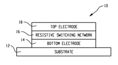
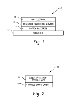
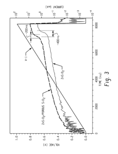
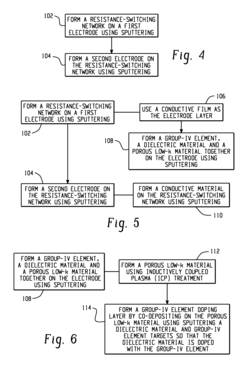
- Incorporating a porous low-k layer and a group-IV element doping layer in the resistance-switching network, where the porous low-k layer is prepared by inductively coupled plasma treatment and the group-IV element is doped into a dielectric material, enhances the switching speed and endurance by forming a multi-layer structure between the electrodes.
Fabrication Processes and Scalability Assessment
The fabrication of Resistive RAM (RRAM) devices represents a critical determinant of their performance characteristics and commercial viability. Current manufacturing processes predominantly employ physical vapor deposition (PVD) techniques, including sputtering and atomic layer deposition (ALD), to create the metal-insulator-metal structure that forms the foundation of RRAM cells. These techniques enable precise control over film thickness down to nanometer scales, which is essential for consistent switching behavior.
The integration of RRAM into existing CMOS processes presents both opportunities and challenges. RRAM fabrication typically requires temperatures below 400°C to maintain compatibility with back-end-of-line (BEOL) processing, making it suitable for integration as an embedded memory solution. However, this temperature constraint limits material choices and can impact the crystallinity and defect concentration in the switching layer, affecting device performance and reliability.
Scalability remains a paramount concern for RRAM technology advancement. Current lithographic techniques have demonstrated RRAM cells with dimensions approaching 10nm, with theoretical scaling limits potentially extending below 5nm. This exceptional scaling potential positions RRAM favorably against competing non-volatile memory technologies. The crossbar architecture, in particular, offers a path to achieving ultra-high density memory arrays with 4F² cell size, where F represents the minimum feature size.
Material selection significantly impacts fabrication complexity and scalability. Binary metal oxides like HfOx and TaOx have gained prominence due to their compatibility with standard semiconductor processes and excellent scaling properties. Conversely, complex perovskite materials, while offering superior switching characteristics in some cases, present greater fabrication challenges and may require specialized deposition techniques that limit their scalability.
Yield and uniformity issues represent significant hurdles in RRAM manufacturing. Device-to-device and cycle-to-cycle variations stem from the stochastic nature of filament formation and rupture processes. Advanced process control strategies, including precise oxygen vacancy management through annealing treatments and interface engineering, have shown promise in mitigating these variations. Additionally, the development of multi-layer structures with engineered oxygen scavenging layers has improved switching uniformity.
The economic viability of RRAM technology depends heavily on achieving cost-effective manufacturing at scale. Current cost models suggest that RRAM could achieve competitive cost-per-bit metrics compared to NAND flash, particularly for specialized applications requiring high endurance or radiation hardness. However, this advantage depends on achieving high manufacturing yields and leveraging existing semiconductor fabrication infrastructure to minimize capital expenditure requirements.
Energy Efficiency and Sustainability Considerations
Energy efficiency has emerged as a critical factor in the evaluation and implementation of Resistive RAM (ReRAM) technologies. When comparing different ReRAM materials, power consumption metrics reveal significant variations that directly impact both operational costs and environmental footprint. Silicon oxide-based ReRAM typically demonstrates lower switching energy requirements (10-100 pJ per operation) compared to metal oxide alternatives such as HfOx and TaOx which often require 100-500 pJ per switching event. This energy efficiency advantage translates to reduced heat generation and lower cooling requirements in data center environments.
The sustainability profile of ReRAM materials extends beyond operational energy considerations to encompass the entire lifecycle environmental impact. Hafnium-based compounds, while offering excellent retention characteristics, require energy-intensive extraction and refinement processes. In contrast, titanium oxide materials present a more favorable environmental profile due to greater natural abundance and less energy-intensive processing requirements, though they may sacrifice some performance parameters.
Manufacturing processes for different ReRAM materials demonstrate varying degrees of environmental efficiency. Recent advancements in low-temperature deposition techniques for zinc oxide-based ReRAM have reduced fabrication energy requirements by approximately 35% compared to conventional high-temperature processes. Additionally, innovations in atomic layer deposition methods for tantalum oxide ReRAM have minimized material waste while maintaining performance integrity, representing a significant step toward more sustainable production practices.
The recyclability of ReRAM components varies substantially across material compositions. Silicon-based ReRAM structures generally offer superior end-of-life reclamation potential, with up to 85% of materials potentially recoverable through established semiconductor recycling channels. Conversely, certain rare earth elements used in specialized ReRAM formulations present significant recycling challenges and potential environmental hazards if improperly disposed of.
Longevity and endurance characteristics directly influence the sustainability profile of different ReRAM materials. Materials demonstrating higher endurance cycles, such as certain aluminum oxide compositions achieving 10^12 switching cycles, contribute to extended device lifespans and reduced electronic waste generation. This contrasts with less durable materials that may require more frequent replacement, thereby increasing resource consumption and waste production over time.
Carbon footprint assessments reveal that the production phase accounts for 60-75% of lifetime emissions for most ReRAM technologies, highlighting the importance of material selection and manufacturing optimization. Recent industry initiatives have focused on developing carbon-neutral fabrication facilities specifically for next-generation memory technologies, with several major manufacturers committing to renewable energy transitions for ReRAM production lines by 2025.
Unlock deeper insights with PatSnap Eureka Quick Research — get a full tech report to explore trends and direct your research. Try now!
Generate Your Research Report Instantly with AI Agent
Supercharge your innovation with PatSnap Eureka AI Agent Platform!