

SiC MOSFET Roadmap And Future Technology Trends
SEP 5, 20259 MIN READ
Generate Your Research Report Instantly with AI Agent
PatSnap Eureka helps you evaluate technical feasibility & market potential.
SiC MOSFET Evolution and Development Goals
Silicon Carbide (SiC) MOSFET technology has evolved significantly since its inception in the early 1990s, transitioning from a laboratory curiosity to a commercial reality that is reshaping power electronics. The evolution began with rudimentary devices exhibiting high on-resistance and reliability issues, progressing through several generations of improvements in channel mobility, oxide interface quality, and manufacturing processes.
The first commercial SiC MOSFETs emerged around 2010-2011 with relatively modest performance metrics compared to today's standards. These early devices operated at voltages of 1200V with specific on-resistance values approximately 10 times higher than current generations. Manufacturing yields were low, and costs remained prohibitively high for mass adoption.
By 2015, second-generation devices demonstrated significant improvements in channel mobility through advanced annealing techniques and epitaxial growth processes. This period marked the beginning of SiC MOSFET penetration into niche high-performance applications where the benefits outweighed the cost premium over silicon alternatives.
The current generation of SiC MOSFETs (2020-2023) features dramatically improved performance with specific on-resistance approaching theoretical material limits, enhanced reliability, and substantially reduced manufacturing costs. These improvements have enabled broader market adoption across electric vehicles, renewable energy systems, and industrial power supplies.
Looking forward, the development goals for SiC MOSFET technology are focused on several key dimensions. First, reducing specific on-resistance further through innovative cell structures and improved channel mobility remains a primary objective, with targets approaching 1 mΩ·cm² for 1200V devices by 2025-2027.
Second, enhancing reliability and ruggedness under extreme operating conditions is critical for expanding into more demanding applications. This includes improving short-circuit withstand capability from current levels of 5-10 μs to beyond 20 μs, and enhancing avalanche ruggedness by 50-100%.
Third, scaling manufacturing to 8-inch wafers (from current 6-inch standard) while maintaining quality and yield is essential for continued cost reduction. The industry aims to achieve cost parity with silicon IGBTs on a system level by 2028-2030, which would remove the final barrier to widespread adoption.
Finally, increasing power density through higher temperature operation (targeting 200-250°C junction temperatures) and improved packaging technologies represents a crucial development goal. This will enable more compact power electronic systems with reduced cooling requirements, particularly beneficial for space-constrained applications like automotive powertrains.
The first commercial SiC MOSFETs emerged around 2010-2011 with relatively modest performance metrics compared to today's standards. These early devices operated at voltages of 1200V with specific on-resistance values approximately 10 times higher than current generations. Manufacturing yields were low, and costs remained prohibitively high for mass adoption.
By 2015, second-generation devices demonstrated significant improvements in channel mobility through advanced annealing techniques and epitaxial growth processes. This period marked the beginning of SiC MOSFET penetration into niche high-performance applications where the benefits outweighed the cost premium over silicon alternatives.
The current generation of SiC MOSFETs (2020-2023) features dramatically improved performance with specific on-resistance approaching theoretical material limits, enhanced reliability, and substantially reduced manufacturing costs. These improvements have enabled broader market adoption across electric vehicles, renewable energy systems, and industrial power supplies.
Looking forward, the development goals for SiC MOSFET technology are focused on several key dimensions. First, reducing specific on-resistance further through innovative cell structures and improved channel mobility remains a primary objective, with targets approaching 1 mΩ·cm² for 1200V devices by 2025-2027.
Second, enhancing reliability and ruggedness under extreme operating conditions is critical for expanding into more demanding applications. This includes improving short-circuit withstand capability from current levels of 5-10 μs to beyond 20 μs, and enhancing avalanche ruggedness by 50-100%.
Third, scaling manufacturing to 8-inch wafers (from current 6-inch standard) while maintaining quality and yield is essential for continued cost reduction. The industry aims to achieve cost parity with silicon IGBTs on a system level by 2028-2030, which would remove the final barrier to widespread adoption.
Finally, increasing power density through higher temperature operation (targeting 200-250°C junction temperatures) and improved packaging technologies represents a crucial development goal. This will enable more compact power electronic systems with reduced cooling requirements, particularly beneficial for space-constrained applications like automotive powertrains.
Market Demand Analysis for SiC Power Devices
The Silicon Carbide (SiC) power device market is experiencing unprecedented growth driven by increasing demand for high-efficiency power electronics across multiple industries. Current market valuations place the global SiC power device market at approximately $1.4 billion in 2023, with projections indicating a compound annual growth rate (CAGR) of 34% through 2028, potentially reaching $6.5 billion by the end of the forecast period.
Electric vehicles (EVs) represent the primary demand driver, accounting for nearly 60% of the total SiC power device market. The automotive sector's transition toward electrification has created substantial demand for SiC MOSFETs and diodes in onboard chargers, DC-DC converters, and particularly in main inverters where efficiency gains directly translate to extended vehicle range. Major automotive manufacturers including Tesla, BYD, and Volkswagen have already incorporated SiC technology in their latest EV models.
Industrial applications constitute the second-largest market segment at approximately 20% of total demand. Factory automation, motor drives, and uninterruptible power supplies benefit significantly from SiC's ability to operate at higher switching frequencies and temperatures compared to traditional silicon devices. This segment is expected to grow at 28% CAGR through 2028.
Renewable energy systems, particularly solar inverters and wind power converters, represent another rapidly expanding application area with 15% market share. The superior efficiency of SiC devices directly improves energy harvest rates in these systems, with field tests demonstrating efficiency improvements of 1-3% compared to silicon-based solutions.
Geographically, Asia-Pacific dominates the market with 45% share, led by China's aggressive EV adoption and manufacturing capabilities. North America follows at 30%, with Europe accounting for 20% of global demand. Both regions show strong growth trajectories driven by automotive electrification and renewable energy initiatives.
Price sensitivity remains a significant market factor. Current SiC devices carry a 2-3x price premium over silicon alternatives, though this gap is narrowing as manufacturing scales. Market analysis indicates price elasticity is highest in consumer and some industrial applications, while automotive and high-performance industrial segments demonstrate greater willingness to absorb premium pricing for performance benefits.
Supply chain constraints present both challenges and opportunities. Limited wafer supply and specialized manufacturing requirements have created bottlenecks, prompting major manufacturers to secure long-term supply agreements and invest in vertical integration. These dynamics favor established players with strong supply chain control while creating entry barriers for new market participants.
Electric vehicles (EVs) represent the primary demand driver, accounting for nearly 60% of the total SiC power device market. The automotive sector's transition toward electrification has created substantial demand for SiC MOSFETs and diodes in onboard chargers, DC-DC converters, and particularly in main inverters where efficiency gains directly translate to extended vehicle range. Major automotive manufacturers including Tesla, BYD, and Volkswagen have already incorporated SiC technology in their latest EV models.
Industrial applications constitute the second-largest market segment at approximately 20% of total demand. Factory automation, motor drives, and uninterruptible power supplies benefit significantly from SiC's ability to operate at higher switching frequencies and temperatures compared to traditional silicon devices. This segment is expected to grow at 28% CAGR through 2028.
Renewable energy systems, particularly solar inverters and wind power converters, represent another rapidly expanding application area with 15% market share. The superior efficiency of SiC devices directly improves energy harvest rates in these systems, with field tests demonstrating efficiency improvements of 1-3% compared to silicon-based solutions.
Geographically, Asia-Pacific dominates the market with 45% share, led by China's aggressive EV adoption and manufacturing capabilities. North America follows at 30%, with Europe accounting for 20% of global demand. Both regions show strong growth trajectories driven by automotive electrification and renewable energy initiatives.
Price sensitivity remains a significant market factor. Current SiC devices carry a 2-3x price premium over silicon alternatives, though this gap is narrowing as manufacturing scales. Market analysis indicates price elasticity is highest in consumer and some industrial applications, while automotive and high-performance industrial segments demonstrate greater willingness to absorb premium pricing for performance benefits.
Supply chain constraints present both challenges and opportunities. Limited wafer supply and specialized manufacturing requirements have created bottlenecks, prompting major manufacturers to secure long-term supply agreements and invest in vertical integration. These dynamics favor established players with strong supply chain control while creating entry barriers for new market participants.
Current Status and Technical Challenges of SiC MOSFET
Silicon Carbide (SiC) MOSFET technology has emerged as a revolutionary advancement in power electronics, offering significant advantages over traditional silicon-based devices. Currently, SiC MOSFETs are commercially available from multiple manufacturers with voltage ratings ranging from 650V to 1700V, with some specialized devices reaching up to 3300V for high-power applications.
The global market adoption of SiC MOSFETs has accelerated significantly in recent years, particularly in electric vehicles, renewable energy systems, and industrial power supplies. Major automotive manufacturers have integrated SiC power modules into their latest EV models, demonstrating the technology's transition from niche applications to mainstream adoption.
Despite this progress, SiC MOSFET technology faces several critical technical challenges. The most significant issue remains the quality of the SiC/SiO2 interface, which exhibits higher defect densities compared to silicon devices. These interface traps lead to reduced channel mobility, threshold voltage instability, and reliability concerns under high-temperature operation.
Channel mobility in SiC MOSFETs typically reaches only 15-40 cm²/V·s, substantially lower than the theoretical potential of the material. This limitation directly impacts on-resistance and overall device efficiency. Various approaches including post-oxidation annealing in nitric oxide (NO) or nitrous oxide (N2O) have shown improvements but have not fully resolved the issue.
Manufacturing challenges persist in substrate quality and wafer size. While 6-inch SiC wafers are now standard in production, the industry lags behind silicon's 12-inch wafers, resulting in higher per-unit costs. Crystal defects such as basal plane dislocations, micropipes, and stacking faults continue to affect yield rates and long-term device reliability.
Packaging technology represents another significant challenge, as SiC devices operate at higher temperatures and switching frequencies than silicon counterparts. Traditional packaging materials and techniques often cannot fully exploit SiC's thermal and electrical capabilities, creating a bottleneck in system-level performance.
The cost of SiC MOSFETs remains 2-3 times higher than equivalent silicon devices, presenting a market adoption barrier despite performance advantages. This cost differential stems from complex manufacturing processes, lower yields, and smaller production volumes compared to mature silicon technology.
Reliability testing standards specifically designed for SiC devices are still evolving. The unique failure mechanisms and operational characteristics of SiC MOSFETs require specialized testing protocols beyond those established for silicon devices, particularly for high-temperature and high-voltage applications.
Addressing these technical challenges requires coordinated efforts across material science, device physics, manufacturing processes, and application engineering to fully realize the potential of SiC MOSFET technology and accelerate its adoption across broader market segments.
The global market adoption of SiC MOSFETs has accelerated significantly in recent years, particularly in electric vehicles, renewable energy systems, and industrial power supplies. Major automotive manufacturers have integrated SiC power modules into their latest EV models, demonstrating the technology's transition from niche applications to mainstream adoption.
Despite this progress, SiC MOSFET technology faces several critical technical challenges. The most significant issue remains the quality of the SiC/SiO2 interface, which exhibits higher defect densities compared to silicon devices. These interface traps lead to reduced channel mobility, threshold voltage instability, and reliability concerns under high-temperature operation.
Channel mobility in SiC MOSFETs typically reaches only 15-40 cm²/V·s, substantially lower than the theoretical potential of the material. This limitation directly impacts on-resistance and overall device efficiency. Various approaches including post-oxidation annealing in nitric oxide (NO) or nitrous oxide (N2O) have shown improvements but have not fully resolved the issue.
Manufacturing challenges persist in substrate quality and wafer size. While 6-inch SiC wafers are now standard in production, the industry lags behind silicon's 12-inch wafers, resulting in higher per-unit costs. Crystal defects such as basal plane dislocations, micropipes, and stacking faults continue to affect yield rates and long-term device reliability.
Packaging technology represents another significant challenge, as SiC devices operate at higher temperatures and switching frequencies than silicon counterparts. Traditional packaging materials and techniques often cannot fully exploit SiC's thermal and electrical capabilities, creating a bottleneck in system-level performance.
The cost of SiC MOSFETs remains 2-3 times higher than equivalent silicon devices, presenting a market adoption barrier despite performance advantages. This cost differential stems from complex manufacturing processes, lower yields, and smaller production volumes compared to mature silicon technology.
Reliability testing standards specifically designed for SiC devices are still evolving. The unique failure mechanisms and operational characteristics of SiC MOSFETs require specialized testing protocols beyond those established for silicon devices, particularly for high-temperature and high-voltage applications.
Addressing these technical challenges requires coordinated efforts across material science, device physics, manufacturing processes, and application engineering to fully realize the potential of SiC MOSFET technology and accelerate its adoption across broader market segments.
Current SiC MOSFET Design and Manufacturing Solutions
01 SiC MOSFET Structure and Fabrication
Silicon Carbide (SiC) MOSFETs feature unique structural designs and fabrication methods that enhance their performance characteristics. These devices typically include specialized gate structures, channel formations, and doping profiles that optimize electron mobility and reduce on-resistance. Advanced fabrication techniques address challenges specific to SiC materials, such as interface quality improvement and defect reduction during epitaxial growth. These structural innovations enable SiC MOSFETs to operate efficiently at high voltages and temperatures.- SiC MOSFET Structure and Fabrication: Silicon Carbide (SiC) MOSFETs feature unique structural designs and fabrication methods that enhance their performance characteristics. These devices typically include specialized gate structures, channel formations, and doping profiles that contribute to their high-voltage handling capabilities. The fabrication process often involves specific thermal oxidation techniques, ion implantation methods, and annealing processes to optimize the SiC/oxide interface quality, which is critical for device reliability and performance.
- Power Conversion and Circuit Applications: SiC MOSFETs are widely implemented in power conversion systems due to their superior switching characteristics and high-temperature operation capabilities. These devices enable more efficient power conversion in applications such as inverters, converters, and motor drives. Circuit designs incorporating SiC MOSFETs often feature specialized gate driving techniques, protection mechanisms, and thermal management solutions to fully leverage the advantages of these wide bandgap semiconductor devices while ensuring reliable operation under various load conditions.
- Thermal Management and Packaging Solutions: Effective thermal management is crucial for SiC MOSFETs due to their high power density and operating temperatures. Advanced packaging technologies have been developed specifically for these devices, including direct bonded copper (DBC) substrates, advanced die-attach materials, and innovative cooling solutions. These packaging approaches aim to minimize thermal resistance, reduce parasitic inductances, and enhance overall reliability, allowing SiC MOSFETs to operate at their full potential while maintaining long-term stability under demanding conditions.
- Reliability Enhancement and Defect Mitigation: Improving the reliability of SiC MOSFETs involves addressing specific challenges such as threshold voltage instability, gate oxide integrity, and body diode performance. Various techniques have been developed to mitigate these issues, including specialized passivation layers, interface treatments, and optimized device architectures. These approaches aim to reduce defect densities at the SiC/oxide interface, enhance channel mobility, and improve long-term stability under various stress conditions, ultimately extending the operational lifetime of SiC MOSFET devices.
- Advanced SiC MOSFET Innovations: Recent innovations in SiC MOSFET technology include novel device structures such as trench designs, super-junction architectures, and specialized field plate configurations. These advancements aim to further reduce on-resistance, increase breakdown voltage, and improve switching performance. Additionally, emerging approaches incorporate heterogeneous integration with other semiconductor materials, advanced epitaxial growth techniques, and innovative doping methods to overcome traditional limitations and push the boundaries of SiC MOSFET performance for next-generation power electronics applications.
02 Thermal Management and Packaging Solutions
Effective thermal management is critical for SiC MOSFETs due to their high-power density operation. Advanced packaging technologies incorporate innovative heat dissipation structures, thermally conductive materials, and optimized layouts to manage junction temperatures. These solutions may include specialized die-attach materials, integrated cooling systems, and thermally optimized substrate designs. Proper thermal management extends device lifetime, maintains performance parameters, and enables reliable operation under extreme conditions.Expand Specific Solutions03 Gate Drive and Control Circuitry
SiC MOSFETs require specialized gate drive circuits to fully leverage their switching capabilities while ensuring reliable operation. These circuits address the unique gate voltage requirements, switching speeds, and parasitic effects associated with SiC technology. Advanced gate drivers incorporate features such as adjustable slew rates, protection against voltage spikes, and temperature compensation. Proper gate control enables optimal switching performance, minimizes losses, and protects against device failure under various operating conditions.Expand Specific Solutions04 Power Conversion Applications
SiC MOSFETs enable significant improvements in power conversion systems across various applications. Their implementation in inverters, converters, and power supplies results in higher efficiency, reduced size, and improved thermal performance. These devices are particularly valuable in renewable energy systems, electric vehicle powertrains, industrial drives, and grid infrastructure where high efficiency and power density are critical. The fast switching capabilities and low losses of SiC MOSFETs allow for higher operating frequencies, smaller passive components, and more compact system designs.Expand Specific Solutions05 Reliability Enhancement and Failure Mechanisms
Understanding and addressing reliability challenges is essential for widespread adoption of SiC MOSFETs. Research focuses on identifying and mitigating failure mechanisms such as threshold voltage instability, gate oxide degradation, and body diode reliability. Advanced testing methodologies, lifetime models, and robustness enhancement techniques have been developed to ensure long-term stable operation. Innovations in this area include improved passivation layers, optimized field distribution structures, and stress-relieving designs that extend device lifetime under harsh operating conditions.Expand Specific Solutions
Key Players in SiC Semiconductor Industry
The SiC MOSFET market is currently in a growth phase, transitioning from early adoption to mainstream implementation, with the global market expected to reach $2.5 billion by 2027, growing at a CAGR of approximately 30%. Technologically, SiC MOSFETs have reached commercial maturity for 650V-1700V applications, with 3300V devices emerging for high-power systems. Key players include established semiconductor manufacturers like Sumitomo Electric, Applied Materials, and Hitachi, alongside specialized SiC-focused companies such as Global Power Technology and GTA Semiconductor. Chinese entities including Huawei Digital Power, Yangjie Electronic, and Shanghai Lanxin are rapidly advancing their capabilities, supported by research partnerships with institutions like Xi'an Jiaotong University and University of Electronic Science & Technology of China, indicating a strategic national focus on developing domestic SiC supply chains.
Yangzhou Yangjie Electronic Technology Co., Ltd.
Technical Solution: Yangjie Electronic has developed a comprehensive SiC MOSFET technology platform targeting medium-voltage applications from 650V to 1700V. Their roadmap focuses on reducing specific on-resistance through advanced cell designs and improved channel mobility. The company has implemented specialized annealing techniques that reduce interface trap density at the SiC/SiO2 interface by approximately 40% compared to conventional processes, resulting in enhanced channel mobility and reduced threshold voltage shift under high-temperature operation. Yangjie's latest generation devices feature optimized JFET regions that balance conduction and switching performance, achieving RDS(on) values below 80mΩ·cm² for 1200V rated devices. Their future technology trends include development of SiC trench MOSFET structures with reduced cell pitch, targeting specific on-resistance reduction of 30% compared to current planar designs, while maintaining short-circuit withstand capability exceeding 5μs at rated current and voltage conditions.
Strengths: Strong domestic supply chain integration within China's semiconductor ecosystem; competitive pricing strategy enabling broader market adoption; rapidly expanding manufacturing capacity. Weaknesses: Less established brand recognition in international markets; limited experience with automotive-grade qualification processes; smaller R&D resources compared to global semiconductor giants.
Huawei Digital Power Technologies Co Ltd
Technical Solution: Huawei Digital Power has developed advanced SiC MOSFET technology specifically optimized for high-efficiency power conversion in telecommunications infrastructure and renewable energy applications. Their roadmap emphasizes system-level optimization through co-design of power devices and control algorithms. Huawei's SiC MOSFETs feature specialized cell structures with reduced Miller capacitance, enabling switching frequencies exceeding 100kHz while maintaining high efficiency. The company has implemented proprietary surface treatment techniques that improve channel mobility by approximately 25% compared to conventional processes, resulting in reduced conduction losses. Their devices incorporate advanced termination structures that achieve over 90% of the theoretical breakdown voltage while minimizing die area. Huawei's future technology trends include development of intelligent power modules with integrated temperature and current sensing capabilities, enabling dynamic performance optimization and predictive maintenance in mission-critical applications.
Strengths: Vertical integration with end applications providing deep system-level optimization capabilities; strong position in telecommunications power infrastructure; extensive experience with high-reliability applications. Weaknesses: Limited external sales channels for semiconductor components; relatively recent entry into semiconductor manufacturing; potential market access challenges in some regions due to geopolitical factors.
Core Patents and Technical Innovations in SiC MOSFET
Silicon carbide field-effect transistors
PatentActiveUS11894454B2
Innovation
- The development of a silicon carbide (SiC) metal-oxide-semiconductor field-effect transistor (MOSFET) with a gate structure comprising a gate oxide layer, an aluminum nitride layer, and a p-type gallium nitride layer, which includes a lateral built-in channel with a p-type AlGaN gate and an AlN buffer layer, providing high threshold voltage and low interface trap density, enabling efficient operation with low on-state resistance.
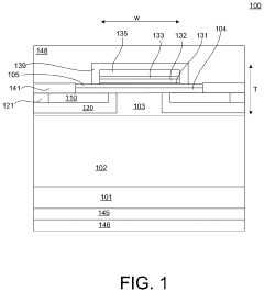
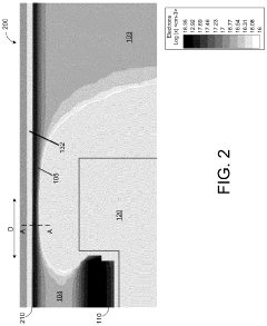
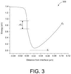
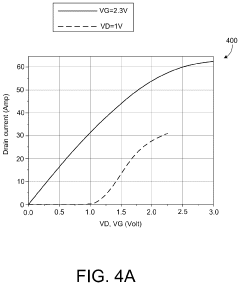
Silicon carbide semiconductor device
PatentPendingUS20240136436A1
Innovation
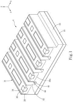
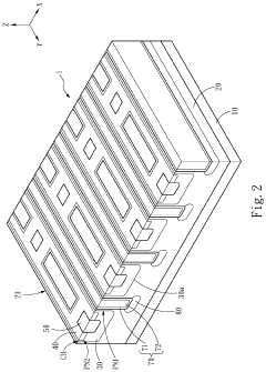
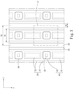
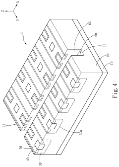
- A silicon carbide semiconductor device with a hybrid gate structure, featuring a trench structure that reduces JFET resistance and parasitic gate-to-drain capacitance, and increases channel width density, comprising a SiC substrate, drift layer, doped regions, and a gate electrode with a trench gate configuration that forms accumulation layers for low resistance current paths.
Supply Chain Analysis for SiC Materials and Components
The SiC MOSFET supply chain represents a complex ecosystem that has evolved significantly in recent years to support the growing demand for wide bandgap semiconductor devices. The supply chain begins with raw silicon carbide material production, which requires specialized manufacturing processes including crystal growth through physical vapor transport (PVT) methods. Currently, this segment is dominated by a few key players including Wolfspeed, II-VI Incorporated, and ROHM, who collectively control approximately 70% of the global SiC substrate market.
The midstream segment of the supply chain involves wafer processing, epitaxy growth, and device fabrication. This area has seen substantial investment as companies work to scale production capacity to meet automotive and industrial power electronics demands. Notable developments include Wolfspeed's Mohawk Valley Fab in New York, which represents a $1 billion investment in 200mm SiC wafer production capabilities. Similarly, STMicroelectronics has expanded its facilities in Italy and Singapore to support vertical integration of its SiC supply chain.
Component manufacturing represents another critical link, where fabricated SiC dies are packaged into modules suitable for end applications. This segment faces unique challenges due to SiC's higher operating temperatures and switching speeds compared to silicon devices. Companies like Infineon, ON Semiconductor, and Mitsubishi Electric have developed specialized packaging solutions to address these requirements, including silver sintering and copper clip bonding technologies.
Regional distribution of the SiC supply chain shows concentration in North America, Europe, and Japan for substrate production, while China has been rapidly expanding its presence across all segments through both domestic companies and foreign investments. The Chinese government's "Third Generation Semiconductor Development Plan" specifically targets SiC technology as a strategic priority, providing significant subsidies and research funding.
Supply chain vulnerabilities include high concentration of raw material production, long lead times for substrate manufacturing (typically 3-6 months), and equipment specialization requirements. These factors have led to strategic vertical integration efforts by major players seeking to secure reliable material sources and production capacity. For example, automotive OEMs like Tesla and major tier-one suppliers have established long-term supply agreements with SiC manufacturers to ensure component availability for electric vehicle production.
Recent global disruptions have highlighted the need for supply chain resilience, prompting geographic diversification of manufacturing capabilities and increased inventory management strategies throughout the ecosystem. As SiC MOSFET adoption accelerates in applications ranging from electric vehicles to renewable energy systems, continued evolution of this supply chain will be critical to supporting industry growth projections of 30% CAGR through 2028.
The midstream segment of the supply chain involves wafer processing, epitaxy growth, and device fabrication. This area has seen substantial investment as companies work to scale production capacity to meet automotive and industrial power electronics demands. Notable developments include Wolfspeed's Mohawk Valley Fab in New York, which represents a $1 billion investment in 200mm SiC wafer production capabilities. Similarly, STMicroelectronics has expanded its facilities in Italy and Singapore to support vertical integration of its SiC supply chain.
Component manufacturing represents another critical link, where fabricated SiC dies are packaged into modules suitable for end applications. This segment faces unique challenges due to SiC's higher operating temperatures and switching speeds compared to silicon devices. Companies like Infineon, ON Semiconductor, and Mitsubishi Electric have developed specialized packaging solutions to address these requirements, including silver sintering and copper clip bonding technologies.
Regional distribution of the SiC supply chain shows concentration in North America, Europe, and Japan for substrate production, while China has been rapidly expanding its presence across all segments through both domestic companies and foreign investments. The Chinese government's "Third Generation Semiconductor Development Plan" specifically targets SiC technology as a strategic priority, providing significant subsidies and research funding.
Supply chain vulnerabilities include high concentration of raw material production, long lead times for substrate manufacturing (typically 3-6 months), and equipment specialization requirements. These factors have led to strategic vertical integration efforts by major players seeking to secure reliable material sources and production capacity. For example, automotive OEMs like Tesla and major tier-one suppliers have established long-term supply agreements with SiC manufacturers to ensure component availability for electric vehicle production.
Recent global disruptions have highlighted the need for supply chain resilience, prompting geographic diversification of manufacturing capabilities and increased inventory management strategies throughout the ecosystem. As SiC MOSFET adoption accelerates in applications ranging from electric vehicles to renewable energy systems, continued evolution of this supply chain will be critical to supporting industry growth projections of 30% CAGR through 2028.
Sustainability and Environmental Impact of SiC Technology
Silicon Carbide (SiC) technology represents a significant advancement in power electronics with substantial environmental benefits compared to traditional silicon-based devices. The sustainability advantages of SiC MOSFETs stem primarily from their superior energy efficiency, which translates to reduced power consumption across various applications. When implemented in electric vehicles, renewable energy systems, and industrial power supplies, SiC devices can achieve energy savings of 5-10% compared to silicon alternatives, resulting in meaningful reductions in carbon emissions over product lifecycles.
The environmental impact assessment of SiC technology must consider the complete lifecycle, from raw material extraction through manufacturing to end-of-life disposal. While SiC manufacturing processes currently require approximately 30% more energy than traditional silicon processing due to higher temperature requirements (typically above 1600°C versus 1400°C for silicon), this initial carbon investment is typically recovered within 1-3 years of operation through improved efficiency.
Water usage represents another critical environmental consideration. SiC wafer production consumes approximately 2,000-3,000 gallons of ultra-pure water per wafer, comparable to silicon manufacturing. However, industry leaders like Wolfspeed and STMicroelectronics have implemented closed-loop water recycling systems that reduce freshwater consumption by up to 40%, establishing new sustainability benchmarks for the sector.
The durability of SiC devices further enhances their environmental profile. With demonstrated lifespans exceeding 15 years in demanding applications and superior performance at high temperatures, SiC MOSFETs require less frequent replacement than silicon alternatives. This longevity reduces electronic waste generation and conserves resources associated with manufacturing replacement components.
Looking forward, the SiC industry is developing more sustainable manufacturing techniques. Innovations include lower-temperature epitaxial growth processes that could reduce energy requirements by 15-20%, and more efficient substrate utilization that may increase the number of devices per wafer by up to 25%. Additionally, research into recycling methods for SiC materials shows promise for creating a more circular economy approach to device manufacturing.
The net environmental impact of widespread SiC adoption appears strongly positive. Analysis indicates that if SiC MOSFETs achieved 50% market penetration in power electronics by 2030, global energy savings could reach approximately 25-30 TWh annually, equivalent to removing 3-4 million cars from roads in terms of carbon emissions reduction. This positions SiC technology as a key enabler for meeting international climate goals while supporting the continued growth of electrification across multiple sectors.
The environmental impact assessment of SiC technology must consider the complete lifecycle, from raw material extraction through manufacturing to end-of-life disposal. While SiC manufacturing processes currently require approximately 30% more energy than traditional silicon processing due to higher temperature requirements (typically above 1600°C versus 1400°C for silicon), this initial carbon investment is typically recovered within 1-3 years of operation through improved efficiency.
Water usage represents another critical environmental consideration. SiC wafer production consumes approximately 2,000-3,000 gallons of ultra-pure water per wafer, comparable to silicon manufacturing. However, industry leaders like Wolfspeed and STMicroelectronics have implemented closed-loop water recycling systems that reduce freshwater consumption by up to 40%, establishing new sustainability benchmarks for the sector.
The durability of SiC devices further enhances their environmental profile. With demonstrated lifespans exceeding 15 years in demanding applications and superior performance at high temperatures, SiC MOSFETs require less frequent replacement than silicon alternatives. This longevity reduces electronic waste generation and conserves resources associated with manufacturing replacement components.
Looking forward, the SiC industry is developing more sustainable manufacturing techniques. Innovations include lower-temperature epitaxial growth processes that could reduce energy requirements by 15-20%, and more efficient substrate utilization that may increase the number of devices per wafer by up to 25%. Additionally, research into recycling methods for SiC materials shows promise for creating a more circular economy approach to device manufacturing.
The net environmental impact of widespread SiC adoption appears strongly positive. Analysis indicates that if SiC MOSFETs achieved 50% market penetration in power electronics by 2030, global energy savings could reach approximately 25-30 TWh annually, equivalent to removing 3-4 million cars from roads in terms of carbon emissions reduction. This positions SiC technology as a key enabler for meeting international climate goals while supporting the continued growth of electrification across multiple sectors.
Unlock deeper insights with PatSnap Eureka Quick Research — get a full tech report to explore trends and direct your research. Try now!
Generate Your Research Report Instantly with AI Agent
Supercharge your innovation with PatSnap Eureka AI Agent Platform!