Strategic Applications of Resistive RAM in Industry
OCT 9, 20259 MIN READ
Generate Your Research Report Instantly with AI Agent
Patsnap Eureka helps you evaluate technical feasibility & market potential.
ReRAM Technology Background and Objectives
Resistive Random Access Memory (ReRAM) represents a significant advancement in non-volatile memory technology, emerging as a promising alternative to traditional memory solutions. The evolution of ReRAM can be traced back to the early 2000s when researchers began exploring the potential of resistance switching phenomena in various metal oxide materials. This technology has since progressed through multiple generations, with each iteration addressing previous limitations in terms of endurance, retention, and switching speed.
The fundamental principle behind ReRAM involves the formation and disruption of conductive filaments within an insulating layer, allowing for binary data storage through high and low resistance states. This mechanism offers several inherent advantages over conventional memory technologies, including lower power consumption, faster switching speeds, and enhanced scalability potential.
Market trends indicate a growing demand for more efficient memory solutions, particularly in data-intensive applications where traditional DRAM and NAND flash technologies face scaling challenges. ReRAM positions itself at the intersection of these established technologies, potentially offering the speed advantages of DRAM with the non-volatility of flash memory.
The global push toward edge computing, Internet of Things (IoT), and artificial intelligence applications has further accelerated interest in ReRAM technology. These applications require memory solutions that can process data efficiently at the point of collection, reducing latency and power consumption associated with cloud-based processing.
Current technical objectives for ReRAM development focus on several key areas: improving cycling endurance to compete with established memory technologies, enhancing data retention capabilities particularly at elevated temperatures, reducing cell-to-cell variability for reliable large-scale array operation, and developing cost-effective manufacturing processes compatible with existing semiconductor fabrication infrastructure.
Industry projections suggest that ReRAM could potentially address the growing "memory wall" challenge—the widening gap between processor and memory performance that increasingly bottlenecks computing systems. By providing faster access times and lower energy requirements than conventional storage technologies, ReRAM may enable new computing architectures that overcome these limitations.
The strategic importance of ReRAM extends beyond consumer electronics into critical sectors including automotive systems, industrial automation, aerospace applications, and medical devices—all areas where reliable non-volatile memory with rapid access times and low power consumption provides significant competitive advantages.
Market Demand Analysis for ReRAM Solutions
The global market for Resistive Random Access Memory (ReRAM) solutions is experiencing significant growth, driven by increasing demands for more efficient, high-performance, and low-power memory technologies. Current market projections indicate that the ReRAM market is expected to grow at a compound annual growth rate of 16% between 2023 and 2030, with the market value anticipated to reach $1.2 billion by 2030.
The primary market demand for ReRAM stems from the data center sector, where the need for faster, more energy-efficient storage solutions continues to escalate. Data centers currently consume approximately 1-2% of global electricity, with memory operations accounting for a substantial portion of this energy usage. ReRAM's non-volatile nature and lower power consumption present a compelling value proposition for data center operators seeking to reduce operational costs and carbon footprints.
In the consumer electronics segment, the demand for ReRAM is being fueled by the growing complexity of mobile applications and the increasing adoption of edge computing. Smartphone manufacturers are particularly interested in ReRAM's potential to extend battery life while maintaining high performance for data-intensive applications. Market research indicates that approximately 30% of next-generation smartphones could incorporate some form of ReRAM technology by 2028.
The automotive industry represents another significant market for ReRAM solutions, particularly with the rise of autonomous vehicles and advanced driver-assistance systems (ADAS). These applications require memory technologies that can operate reliably in extreme conditions while processing vast amounts of sensor data in real-time. The automotive memory market is projected to grow by 25% annually through 2027, with ReRAM positioned to capture an increasing share.
Industrial IoT applications are also driving demand for ReRAM, as manufacturers deploy more sensors and edge computing devices throughout their operations. The industrial sector values ReRAM's durability, with endurance ratings exceeding 10^6 cycles, significantly outperforming traditional flash memory. Market analysts predict that industrial applications could account for 22% of the total ReRAM market by 2026.
The healthcare sector is emerging as a promising market for ReRAM solutions, particularly in medical imaging and wearable health monitoring devices. These applications benefit from ReRAM's combination of high speed, low power consumption, and radiation hardness. The medical electronics market is growing at 15% annually, with memory components representing a critical segment within this expansion.
Despite these positive trends, market adoption faces challenges related to cost competitiveness against established technologies like DRAM and NAND flash. Current ReRAM solutions remain approximately 30-40% more expensive per gigabyte than mainstream alternatives, though this gap is expected to narrow as manufacturing scales increase and processes mature.
ReRAM Development Status and Technical Challenges
Resistive RAM (ReRAM) technology has reached a critical juncture in its development trajectory, with significant advancements achieved alongside persistent technical challenges. Currently, ReRAM devices demonstrate promising performance metrics, including switching speeds in the nanosecond range, endurance cycles of 10^6-10^9, and retention times exceeding 10 years at elevated temperatures. These characteristics position ReRAM as a competitive alternative to conventional memory technologies.
The global landscape of ReRAM development shows concentration in three primary regions: North America, East Asia, and Europe. Companies and research institutions in these areas have established distinct approaches to overcoming the technology's fundamental challenges. North American entities typically focus on materials innovation and system integration, while East Asian organizations emphasize manufacturing scalability and cost reduction. European research centers often concentrate on reliability enhancement and specialized applications.
Despite promising progress, ReRAM faces several significant technical hurdles. Variability in switching behavior remains a primary concern, with device-to-device and cycle-to-cycle variations impacting reliability and yield rates. This inconsistency stems from the stochastic nature of filament formation and rupture processes within the resistive switching layer. Current manufacturing processes struggle to achieve the precise control needed for consistent performance across large arrays.
Endurance limitations present another substantial challenge. While certain ReRAM configurations demonstrate impressive cycling capabilities, these often come at the expense of other performance parameters such as retention time or operating voltage. The trade-off between endurance and other critical metrics continues to constrain ReRAM's applicability in write-intensive applications.
The sneak path current problem in crossbar architectures represents a significant obstacle to high-density integration. Without effective selector devices or alternative array architectures, parasitic currents through unselected cells limit the practical size of ReRAM arrays. Various selector technologies are under investigation, including threshold switching devices and complementary resistive switches, but each introduces additional complexity and potential compatibility issues.
Power consumption during the SET operation remains higher than desired for many mobile and IoT applications. The current required to form conductive filaments necessitates careful power management strategies, particularly in battery-operated devices. Research efforts are increasingly focused on reducing the energy requirements for switching operations while maintaining performance reliability.
Scaling challenges become more pronounced as ReRAM moves toward advanced technology nodes. At dimensions below 20nm, quantum effects and material interface phenomena introduce new variables that affect switching behavior. The physics of resistive switching at these scales requires further fundamental understanding to enable predictable device performance.
Current ReRAM Implementation Strategies
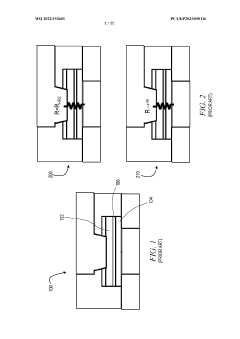
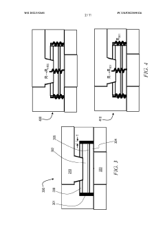
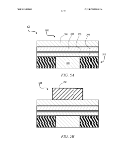
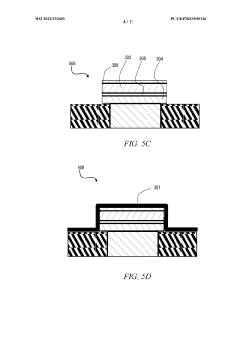
01 Materials and structures for RRAM devices
Resistive Random Access Memory (RRAM) devices utilize specific materials and structures to achieve resistive switching behavior. These typically include metal oxides like HfO2, TiO2, or Ta2O5 as the switching layer sandwiched between two electrodes. The structure may incorporate additional layers such as barrier layers or doping elements to enhance performance. The specific arrangement and composition of these materials significantly impact the device's switching characteristics, endurance, and retention properties.- Resistive RAM device structures: Resistive RAM (RRAM) devices are typically structured with a resistive switching material sandwiched between two electrodes. Various device architectures have been developed, including crossbar arrays, 3D stacking configurations, and integration with transistors for improved performance. These structures aim to optimize memory density, reduce power consumption, and enhance switching reliability. The design of these structures plays a crucial role in determining the overall performance characteristics of RRAM technology.
- Resistive switching materials: The choice of resistive switching materials is fundamental to RRAM operation. Common materials include metal oxides (such as HfOx, TaOx, TiOx), chalcogenides, and perovskites. These materials exhibit controllable resistance changes when subjected to electrical stimuli. The composition, deposition method, and defect engineering of these materials significantly impact switching characteristics, endurance, and retention time. Research focuses on developing materials with optimal switching properties while maintaining compatibility with standard semiconductor manufacturing processes.
- Operation mechanisms and control methods: RRAM devices operate through various resistance switching mechanisms, including filament formation/rupture, interface-type switching, and phase changes. Precise control of set/reset operations is achieved through voltage/current pulse engineering, compliance current techniques, and specialized programming algorithms. These control methods are essential for achieving reliable multi-level cell operation, preventing device degradation, and optimizing the trade-off between switching speed and power consumption. Advanced sensing schemes are also developed to accurately read the resistance states.
- Integration with CMOS technology: Successful integration of RRAM with conventional CMOS technology is crucial for commercial viability. This integration involves addressing challenges related to process compatibility, thermal budgets, and interconnect schemes. Back-end-of-line integration approaches are commonly employed to incorporate RRAM cells into existing semiconductor manufacturing flows. Circuit design considerations include peripheral circuits for addressing, sensing, and programming operations. The co-integration enables the development of hybrid memory systems that leverage the advantages of both technologies.
- Reliability and performance enhancement techniques: Enhancing RRAM reliability involves addressing issues such as endurance degradation, retention loss, and variability between devices. Techniques include doping of switching materials, interface engineering, and optimized electrode materials selection. Pulse shaping methods and adaptive programming schemes help extend device lifetime and improve consistency. Advanced error correction codes and redundancy schemes are implemented at the system level to compensate for device-level variations. These enhancements are essential for meeting the requirements of both storage and computing applications.
02 Switching mechanisms and operation principles
RRAM operation is based on the reversible switching between high and low resistance states through the formation and rupture of conductive filaments within the switching layer. This process is typically controlled by applying appropriate voltage pulses that induce ion migration or oxygen vacancy movement. Different switching modes exist, including unipolar and bipolar switching, depending on the polarity requirements for SET and RESET operations. Understanding these mechanisms is crucial for optimizing device performance and reliability.Expand Specific Solutions03 Integration and fabrication techniques
Fabrication of RRAM devices involves various deposition techniques such as atomic layer deposition, sputtering, or chemical vapor deposition to create the multi-layer structure. Integration challenges include ensuring compatibility with CMOS processes, minimizing cell size for high density, and maintaining uniformity across large arrays. Advanced patterning methods and 3D stacking approaches are employed to increase memory density while specialized etching and deposition processes help maintain critical material properties during fabrication.Expand Specific Solutions04 Circuit design and array architecture
RRAM array architectures include crossbar arrays, 1T1R (one transistor, one resistor) configurations, and 3D stacking arrangements. These designs address challenges such as sneak path currents, which can cause read disturbances in high-density arrays. Peripheral circuits for RRAM include sense amplifiers for reading the resistance state, write drivers for programming operations, and address decoders. These circuits must be designed to handle the unique electrical characteristics of RRAM devices while minimizing power consumption and area overhead.Expand Specific Solutions05 Reliability enhancement and performance optimization
Improving RRAM reliability involves addressing issues such as resistance state drift, endurance degradation, and variability between cells. Techniques include optimizing programming algorithms with verify operations, implementing error correction codes, and carefully controlling operating conditions. Performance optimization focuses on reducing switching energy, improving switching speed, and enhancing data retention. This may involve material engineering, interface modification, or the introduction of specialized barrier layers to control ion migration and filament formation.Expand Specific Solutions
Key Industry Players in ReRAM Development
The Resistive RAM (ReRAM) market is currently in a growth phase, transitioning from research to commercialization with an estimated market size of $1-2 billion, projected to reach $4-5 billion by 2028. The competitive landscape features established semiconductor giants like Samsung, IBM, Micron, and TSMC alongside specialized players such as CrossBar, Adesto, and Winbond. Technology maturity varies significantly across companies, with IBM, Samsung, and Micron demonstrating advanced ReRAM implementations in commercial products, while KIOXIA and CrossBar lead in patent portfolios and novel architectures. Chinese manufacturers including SMIC and UMC are rapidly advancing their capabilities, particularly for industrial IoT and automotive applications, creating a dynamic competitive environment where strategic partnerships between memory specialists and foundry services are becoming increasingly important.
International Business Machines Corp.
Technical Solution: IBM has developed advanced ReRAM technology as part of their comprehensive research into next-generation memory solutions. Their approach utilizes phase-change materials in a unique confined cell architecture that enhances reliability and reduces variability. IBM's ReRAM implementation features multi-level cell capabilities (4 bits per cell demonstrated) with sophisticated error correction techniques to maintain data integrity[8]. The company has pioneered the integration of ReRAM with conventional CMOS logic, creating hybrid chips that leverage the benefits of both technologies. IBM's ReRAM technology demonstrates switching speeds below 10ns, endurance exceeding 10^7 cycles, and remarkable data retention characteristics (projected >10 years at 85°C)[9]. A key strategic focus for IBM is the application of ReRAM in neuromorphic computing, where they have demonstrated artificial synapses with analog weight updates that closely mimic biological learning mechanisms. Their neuromorphic chips incorporating ReRAM have achieved significant improvements in energy efficiency for AI workloads, with power consumption reduced by up to 280x compared to conventional GPU implementations for certain neural network operations[10].
Strengths: IBM's extensive research capabilities have produced ReRAM designs with exceptional multi-level cell performance and integration with advanced CMOS technology. Their neuromorphic computing implementations represent some of the most advanced applications of ReRAM technology. Weaknesses: IBM's focus on research rather than high-volume manufacturing may slow commercial deployment compared to memory-focused competitors.
KIOXIA Corp.
Technical Solution: KIOXIA (formerly Toshiba Memory) has developed innovative ReRAM technology as part of their memory portfolio diversification strategy. Their approach utilizes a tantalum oxide-based switching layer with proprietary electrode materials that enhance filament formation control and stability. KIOXIA's ReRAM implementation features a crossbar architecture with integrated selector devices that effectively mitigate sneak path currents while maintaining high density. Their technology demonstrates impressive performance metrics, including switching speeds below 50ns, endurance exceeding 10^6 cycles, and low operating voltages (typically 1-2V)[11]. KIOXIA has successfully demonstrated ReRAM arrays with capacities up to 128Gb, positioning the technology as a viable storage class memory solution. A key innovation in KIOXIA's approach is their adaptive programming algorithm that compensates for cell-to-cell variations, significantly improving yield and reliability in large arrays. The company has strategically positioned their ReRAM technology for automotive and industrial applications, where its wide operating temperature range (-40°C to 125°C) and radiation hardness provide significant advantages over conventional flash memory[12].
Strengths: KIOXIA's extensive experience in high-volume memory manufacturing provides significant advantages in scaling ReRAM technology to commercial production. Their technology shows excellent reliability characteristics under extreme environmental conditions. Weaknesses: Their current ReRAM solutions still face challenges with write endurance limitations compared to DRAM, potentially restricting applications in write-intensive workloads.
Critical ReRAM Patents and Technical Innovations
High operating speed resistive random access memory
PatentWO2013177566A1
Innovation
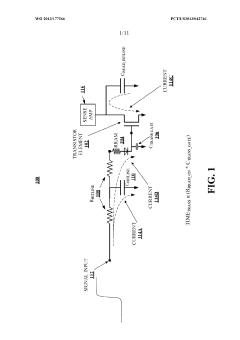
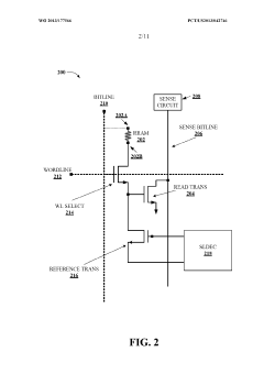
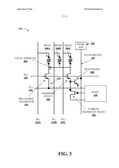
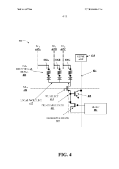
- The development of a high-speed RRAM architecture that connects multiple RRAM devices to a single read transistor, utilizing a reference transistor to apply a bias voltage and mitigate off-current, and employing a sensing circuit to quickly detect changes in electrical characteristics, enabling fast programming, reading, and erasing operations while reducing the number of read transistors and associated circuitry.
Setting an upper bound on RRAM resistance
PatentWO2022152601A1
Innovation
- Incorporating a high-resistance semiconductive spacer in parallel with the RRAM module, using materials like TiOxNy or TaxNy, to provide an upper bound on resistance, ensuring proper operation even with manufacturing defects and enhancing stability by encapsulating the filament layer.
Energy Efficiency and Sustainability Aspects of ReRAM
Resistive RAM (ReRAM) technology presents significant advantages in energy efficiency compared to conventional memory technologies, positioning it as a sustainable solution for future computing systems. The power consumption of ReRAM during operation is substantially lower than that of DRAM and comparable to Flash memory, with standby power requirements approaching zero due to its non-volatile nature. This characteristic eliminates the need for constant refresh operations that consume considerable energy in volatile memory systems.
The manufacturing process of ReRAM also demonstrates environmental benefits. The fabrication requires fewer processing steps and lower thermal budgets compared to conventional memory technologies, resulting in reduced carbon footprint during production. Additionally, the materials used in ReRAM cells, primarily metal oxides, are more abundant and less environmentally harmful than some rare earth elements used in other memory technologies.
From a lifecycle perspective, ReRAM devices offer extended operational lifespans due to their high endurance characteristics, potentially reducing electronic waste generation. The technology's ability to maintain stored information without power consumption contributes to energy conservation in data centers and mobile devices, where memory systems account for a significant portion of total power consumption.
In edge computing applications, ReRAM's energy efficiency becomes particularly valuable. Devices deployed in remote locations or powered by limited energy sources such as batteries or energy harvesting systems benefit from ReRAM's minimal power requirements. This enables longer operational periods between maintenance interventions and reduces the environmental impact associated with battery replacements.
The scalability of ReRAM technology further enhances its sustainability profile. As device dimensions decrease, the energy required for switching operations reduces proportionally, offering a path toward increasingly efficient memory systems. This scaling advantage aligns with the industry's push toward more sustainable computing infrastructures.
Recent advancements in ReRAM design have focused on optimizing energy efficiency through innovative circuit architectures and materials engineering. Techniques such as partial reset operations and adaptive programming schemes have demonstrated potential for further reducing energy consumption during write operations, which traditionally represent the most energy-intensive processes in ReRAM operation.
Looking forward, the integration of ReRAM in neuromorphic computing systems presents additional sustainability benefits. The inherent characteristics of ReRAM cells enable efficient implementation of artificial neural networks with significantly lower energy requirements than conventional computing architectures, potentially revolutionizing the energy efficiency of artificial intelligence applications.
ReRAM Integration with Emerging Computing Paradigms
The integration of Resistive RAM (ReRAM) with emerging computing paradigms represents a transformative frontier in modern computing architectures. ReRAM's unique characteristics—non-volatility, low power consumption, and compatibility with CMOS processes—position it as an ideal candidate for novel computing approaches beyond traditional von Neumann architectures.
Neuromorphic computing systems, which mimic the brain's neural networks, benefit significantly from ReRAM integration. The analog nature of ReRAM cells allows them to function as artificial synapses, enabling efficient implementation of neural network algorithms with significantly reduced power consumption compared to conventional digital approaches. This synergy has accelerated development in edge AI applications where power constraints are critical.
In-memory computing represents another paradigm where ReRAM demonstrates exceptional promise. By performing computational operations directly within memory arrays, ReRAM-based systems can overcome the memory bottleneck that plagues conventional architectures. Early implementations have demonstrated orders of magnitude improvements in energy efficiency for specific workloads, particularly those involving matrix operations common in machine learning applications.
Quantum-inspired computing models have also begun exploring ReRAM integration. While not quantum computing in the strict sense, these hybrid systems leverage ReRAM's ability to maintain multiple resistance states to implement probabilistic computing models that can address optimization problems traditionally targeted by quantum approaches.
Edge computing deployments benefit from ReRAM's non-volatility and low standby power, enabling persistent intelligence in IoT devices. The ability to retain trained models without power consumption addresses a fundamental challenge in distributed intelligence systems, allowing for truly autonomous edge devices that can operate for extended periods on limited power sources.
Security applications have emerged as another integration pathway, with ReRAM-based physical unclonable functions (PUFs) providing hardware-level security primitives. The inherent variability in ReRAM cell characteristics creates unique device signatures that can be leveraged for authentication and encryption key generation.
Challenges remain in standardizing programming models for these emerging paradigms. Traditional software frameworks are ill-suited for the parallel, analog nature of ReRAM-based computing, necessitating new programming abstractions and compiler technologies to fully exploit the hardware capabilities.
As these integration efforts mature, we anticipate the emergence of specialized ReRAM-based computing platforms optimized for specific application domains rather than general-purpose computing, potentially reshaping the computing landscape over the next decade.
Unlock deeper insights with Patsnap Eureka Quick Research — get a full tech report to explore trends and direct your research. Try now!
Generate Your Research Report Instantly with AI Agent
Supercharge your innovation with Patsnap Eureka AI Agent Platform!