Understanding Resistive RAM's Applications in Modern Industries
OCT 9, 20259 MIN READ
Generate Your Research Report Instantly with AI Agent
Patsnap Eureka helps you evaluate technical feasibility & market potential.
ReRAM Technology Background and Objectives
Resistive Random Access Memory (ReRAM) represents a significant advancement in non-volatile memory technology, emerging as a promising alternative to conventional memory solutions. The evolution of ReRAM can be traced back to the early 2000s when researchers began exploring the potential of resistance switching phenomena in various metal oxide materials. This technology has since progressed through multiple development phases, moving from theoretical concepts to practical implementations in specialized applications.
The fundamental principle behind ReRAM involves the formation and disruption of conductive filaments within an insulating layer, allowing for the storage of binary information through resistance states. This mechanism offers several inherent advantages over traditional memory technologies, including lower power consumption, faster switching speeds, and enhanced durability through write cycles.
Recent technological advancements have accelerated ReRAM development, particularly in materials science and fabrication techniques. The integration of novel materials such as hafnium oxide, tantalum oxide, and various perovskite structures has significantly improved device performance and reliability. Concurrently, innovations in manufacturing processes have addressed previous scalability challenges, bringing ReRAM closer to widespread commercial viability.
The global trajectory of ReRAM technology indicates a shift from research-focused development to industry-oriented applications. This transition is evidenced by increasing patent filings from major semiconductor companies and growing investments in ReRAM manufacturing infrastructure. Industry forecasts suggest that the ReRAM market will experience substantial growth over the next decade, driven by emerging applications in edge computing, Internet of Things (IoT) devices, and artificial intelligence systems.
The primary technical objectives for ReRAM development center on addressing several key challenges. These include enhancing retention time and endurance characteristics, improving uniformity across large arrays, reducing operating voltages, and developing more efficient integration methods with conventional CMOS technology. Additionally, there is significant focus on optimizing ReRAM for specific application domains, particularly those requiring low power consumption and high-speed operation.
From an industry perspective, ReRAM aims to establish itself as a viable solution for the growing gap between processing capabilities and memory performance in modern computing systems. The technology seeks to overcome the limitations of current memory hierarchies by offering a combination of non-volatility, high density, and DRAM-like access speeds. This positions ReRAM as a potential enabler for next-generation computing architectures, particularly those designed for data-intensive applications and real-time processing requirements.
Market Demand Analysis for Non-Volatile Memory
The non-volatile memory market has experienced significant growth in recent years, driven by increasing demand for data storage solutions across various industries. The global non-volatile memory market was valued at approximately $67 billion in 2021 and is projected to reach $125 billion by 2028, representing a compound annual growth rate (CAGR) of around 9.3% during the forecast period. This growth is primarily attributed to the rising adoption of Internet of Things (IoT) devices, artificial intelligence applications, and the exponential increase in data generation across sectors.
Resistive RAM (ReRAM) is emerging as a promising technology within the non-volatile memory landscape, offering advantages over traditional solutions like NAND flash and DRAM. Market analysis indicates that ReRAM could capture up to 15% of the overall non-volatile memory market by 2030, particularly in applications requiring high endurance, low power consumption, and fast switching speeds.
The automotive industry represents a significant growth area for non-volatile memory technologies, with connected and autonomous vehicles requiring robust storage solutions for sensor data, navigation systems, and over-the-air updates. The automotive memory market is expected to grow at a CAGR of 23% through 2026, with ReRAM positioned to address specific requirements for reliability in extreme operating conditions.
Consumer electronics continues to be the largest application segment for non-volatile memory, accounting for approximately 40% of market share. Smartphones, tablets, and wearable devices increasingly demand higher storage capacities with lower power consumption, creating opportunities for ReRAM integration. The average storage capacity in smartphones has increased from 64GB to 256GB in recent years, reflecting consumer demand for enhanced data storage capabilities.
Enterprise storage systems and data centers represent another crucial market segment, driven by cloud computing expansion and big data analytics. These applications require memory solutions with high reliability, speed, and endurance – attributes that ReRAM can potentially deliver. The enterprise storage market is projected to grow at a CAGR of 13.5% through 2027, with non-volatile memory playing a central role in this expansion.
Geographically, Asia-Pacific dominates the non-volatile memory market, accounting for approximately 45% of global market share, followed by North America at 30% and Europe at 20%. China, South Korea, and Taiwan are key manufacturing hubs, while North America leads in research and development activities for next-generation memory technologies like ReRAM.
The industrial IoT sector presents substantial growth opportunities for ReRAM, with applications in smart manufacturing, predictive maintenance, and industrial automation. This segment is expected to grow at a CAGR of 16.7% through 2028, creating demand for reliable, low-power memory solutions that can operate in harsh industrial environments.
ReRAM Development Status and Technical Challenges
Resistive RAM (ReRAM) technology has evolved significantly over the past decade, positioning itself as a promising next-generation non-volatile memory solution. Currently, ReRAM development has reached a semi-mature stage with several companies producing commercial prototypes and limited production devices. The technology demonstrates superior characteristics compared to conventional flash memory, including faster switching speeds, lower power consumption, and enhanced endurance cycles.
Despite these advancements, ReRAM faces several critical technical challenges that impede its widespread commercial adoption. The foremost issue is reliability, particularly related to retention time degradation and resistance drift phenomena. These reliability concerns manifest as data loss over time and inconsistent performance across different operating conditions, creating significant barriers for applications requiring long-term data storage.
Scaling challenges represent another major hurdle in ReRAM development. As device dimensions shrink below 20nm, maintaining consistent switching behavior becomes increasingly difficult due to material interface effects and variability in filament formation. This variability leads to unpredictable performance characteristics and yield issues in high-density memory arrays.
The underlying switching mechanism in ReRAM devices remains incompletely understood, complicating efforts to optimize device performance. The complex interplay between electrochemical reactions, thermal effects, and ion migration during switching operations creates challenges in developing accurate models for device behavior prediction and optimization.
Manufacturing integration presents additional obstacles, particularly regarding compatibility with standard CMOS processes. Current fabrication approaches often require specialized materials and processing steps that deviate from established semiconductor manufacturing flows, increasing production costs and limiting scalability.
Geographically, ReRAM technology development exhibits distinct regional characteristics. Asian companies, particularly in Japan, South Korea, and Taiwan, lead in patent filings and commercial development efforts. European research institutions contribute significantly to fundamental understanding of switching mechanisms, while North American companies focus on specialized applications and system-level integration.
The endurance limitations of ReRAM devices (typically 10^6-10^9 cycles) restrict their application in scenarios requiring frequent write operations. This limitation becomes particularly problematic for storage class memory applications that demand both non-volatility and DRAM-like endurance characteristics.
Power consumption during the SET operation remains higher than theoretical limits, creating thermal management challenges in high-density arrays. This issue becomes particularly pronounced in mobile and IoT applications where energy efficiency is paramount.
AI and neuromorphic computing applications present unique challenges for ReRAM implementation, including requirements for precise analog states, symmetrical programming characteristics, and consistent device-to-device behavior. Addressing these specialized requirements necessitates tailored device architectures and materials systems that differ from conventional digital memory applications.
Current ReRAM Implementation Solutions
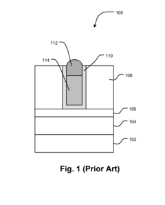
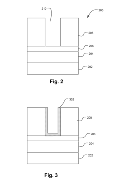
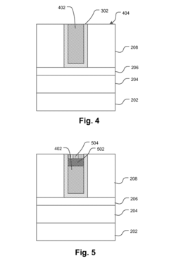
01 Resistive RAM device structures
Resistive RAM (RRAM) devices are constructed with specific structures to enable resistive switching behavior. These structures typically include a resistive switching layer sandwiched between two electrodes. Various materials can be used for the resistive switching layer, such as metal oxides, and different electrode configurations can be employed to optimize device performance. The structural design of RRAM devices affects key parameters like switching speed, endurance, and retention time.- Materials and structures for RRAM devices: Resistive Random Access Memory (RRAM) devices utilize specific materials and structures to enable resistive switching behavior. These typically include metal oxides like HfO2, TiO2, or Ta2O5 as the switching layer sandwiched between two electrodes. The structure may incorporate additional layers such as barrier layers or doping elements to enhance performance. The specific arrangement and composition of these materials significantly impact the device's switching characteristics, endurance, and retention properties.
- Switching mechanisms and operation principles: RRAM devices operate based on resistance switching phenomena where the resistance state can be altered between high resistance state (HRS) and low resistance state (LRS). The switching mechanisms typically involve the formation and rupture of conductive filaments through processes like oxygen vacancy migration, metal ion migration, or phase changes. These mechanisms are controlled by applying appropriate voltage pulses that trigger the physical or chemical changes in the resistive switching layer, enabling data storage through distinct resistance states.
- Integration and fabrication techniques: Fabrication of RRAM devices involves specialized techniques to ensure proper integration with existing semiconductor technologies. This includes deposition methods like atomic layer deposition (ALD), sputtering, or chemical vapor deposition (CVD) for the switching layer, and lithography processes for patterning. Advanced integration approaches may involve 3D stacking, crossbar arrays, or embedding RRAM cells within back-end-of-line (BEOL) processes. These techniques aim to maximize density while maintaining compatibility with CMOS processes.
- Circuit design and peripheral components: RRAM memory arrays require specialized circuit designs and peripheral components to enable reliable operation. These include sense amplifiers for reading the resistance states, write drivers for programming operations, and address decoders for cell selection. Advanced designs may incorporate reference cells, temperature compensation circuits, or adaptive programming schemes to enhance reliability. The peripheral circuitry must address challenges like sneak path currents in crossbar arrays and provide sufficient margins for distinguishing between resistance states.
- Multi-level cell operation and reliability enhancement: Advanced RRAM implementations support multi-level cell (MLC) operation, where multiple resistance states are used to store more than one bit per cell. This requires precise control of the resistance levels and specialized programming algorithms. Reliability enhancement techniques address challenges like resistance drift, endurance limitations, and retention failures through methods such as error correction codes, adaptive programming schemes, or specialized material engineering. These approaches aim to improve the stability and longevity of RRAM devices for practical applications.
02 Materials for resistive switching layers
The choice of materials for the resistive switching layer is crucial for RRAM performance. Metal oxides such as HfOx, TaOx, and TiOx are commonly used due to their favorable switching characteristics. Other materials include chalcogenides, perovskites, and organic compounds. The composition, stoichiometry, and defect concentration in these materials significantly influence the resistive switching mechanism, which can be based on oxygen vacancy migration, metallic filament formation, or phase change phenomena.Expand Specific Solutions03 RRAM array architecture and integration
RRAM devices can be arranged in various array architectures to create memory systems. These include crossbar arrays, 3D stacking configurations, and hybrid designs. Integration challenges involve addressing schemes, selector devices to mitigate sneak path currents, and compatibility with CMOS processes. Advanced architectures aim to increase storage density while maintaining reliable operation and minimizing interference between adjacent cells.Expand Specific Solutions04 Programming and operation methods
RRAM devices require specific programming methods to control the resistive switching process. These include voltage pulse schemes for SET and RESET operations, current compliance techniques to prevent device damage, and verification algorithms to ensure reliable state changes. Advanced operation methods may incorporate adaptive programming, multi-level cell operation for increased storage density, and techniques to mitigate variability and improve endurance.Expand Specific Solutions05 Novel applications of resistive RAM
Beyond conventional memory applications, RRAM technology is being explored for novel uses such as neuromorphic computing, in-memory computing, and security applications. The analog nature of resistive switching makes RRAM suitable for implementing artificial neural networks and synaptic functions. Other applications include physical unclonable functions for security, non-volatile logic circuits, and radiation-hardened memory for space applications.Expand Specific Solutions
Key Industry Players in ReRAM Development
Resistive RAM (ReRAM) technology is currently in the early growth phase of its industry lifecycle, with an estimated market size of $300-400 million that is projected to expand significantly as applications diversify. The competitive landscape features established semiconductor giants like Samsung, SK Hynix, and Micron Technology investing heavily in ReRAM development, alongside specialized players such as CrossBar and Adesto Technologies who are pioneering innovative implementations. IBM and KIOXIA are advancing the technology's integration with conventional memory architectures, while foundries including TSMC, SMIC, and UMC are developing manufacturing processes to scale production. Technical maturity varies across applications, with ReRAM showing particular promise in embedded systems, IoT devices, and neuromorphic computing where its non-volatility, low power consumption, and high density provide competitive advantages over traditional memory technologies.
Micron Technology, Inc.
Technical Solution: Micron has developed a proprietary ReRAM technology called 3D XPoint (initially co-developed with Intel) that offers significant performance advantages over conventional memory solutions. Their ReRAM implementation uses chalcogenide materials in a crosspoint architecture that enables bit-level addressability without the need for transistors at each cell. Micron's solution achieves 1000x better endurance than NAND flash while providing 10x denser storage than conventional DRAM[2]. The company has focused on optimizing their ReRAM for data-intensive applications, achieving read latencies of less than 100 nanoseconds and write operations in under 500 nanoseconds[4]. Micron's ReRAM technology incorporates advanced selector devices that minimize sneak path currents while maintaining high cell density. Their manufacturing approach leverages existing semiconductor fabrication techniques, allowing for cost-effective production scaling and integration with conventional CMOS processes.
Strengths: Extensive experience in memory manufacturing and scaling; established market channels and customer relationships; strong R&D capabilities in materials science. Weaknesses: Faces competition from alternative emerging memory technologies like MRAM and FeRAM; challenges in achieving cost parity with established memory technologies for mainstream adoption.
Samsung Electronics Co., Ltd.
Technical Solution: Samsung has developed advanced ReRAM technology that combines high-density storage capabilities with low power consumption. Their solution integrates ReRAM cells into crossbar array architectures, enabling multi-level cell (MLC) operation that stores multiple bits per cell. Samsung's ReRAM technology employs hafnium oxide-based materials for the resistive switching layer, which provides excellent endurance and retention characteristics[1]. The company has demonstrated ReRAM devices with sub-10nm feature sizes, positioning them for integration with advanced logic processes. Samsung's implementation includes innovative selector devices to minimize sneak path currents in high-density arrays, and they've developed specialized programming algorithms that enhance write/erase cycling reliability while maintaining fast switching speeds[3]. Their ReRAM solutions target both standalone memory applications and embedded applications in IoT, automotive, and AI edge computing devices.
Strengths: Industry-leading manufacturing capabilities allow for rapid scaling and commercialization; extensive IP portfolio in memory technologies; strong vertical integration from materials to systems. Weaknesses: ReRAM technology still faces challenges in long-term reliability and endurance compared to established memory technologies; higher production costs during initial commercialization phases.
Core ReRAM Switching Mechanism Analysis
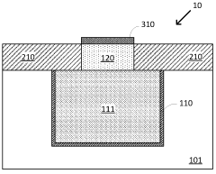
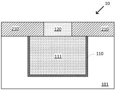
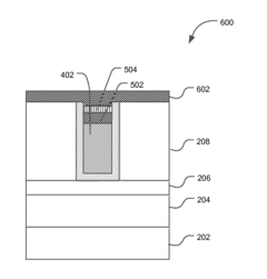
RRAM cell with nonplanar metal oxide layer
PatentWO2024023596A1
Innovation
- A resistive random-access memory (RRAM) cell design featuring a nonplanar metal oxide layer with a central portion directly contacting the bottom electrode and a peripheral portion that is nonplanar, along with a vertical portion between them, reduces the need for high work function metals by using cost-effective materials for the bottom contact stud and selectively depositing high work function metals only on the bottom contact stud, thereby minimizing waste.
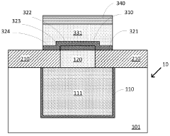
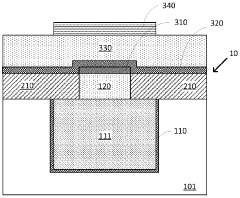
Resistive ram and fabrication method
PatentActiveUS20140264237A1
Innovation
- The method involves forming a nitrogen-containing metal oxide layer, such as tungsten oxynitride, over a transition metal electrode using a rapid thermal oxidation process, which reduces the forming voltage and improves the flatness of the metal oxide surface, facilitating subsequent processing and enhancing device performance by lowering the set and reset voltages.
Energy Efficiency and Sustainability Aspects
Resistive RAM (ReRAM) technology represents a significant advancement in energy-efficient computing solutions. When examining the energy consumption profile of ReRAM compared to conventional memory technologies, the advantages become immediately apparent. ReRAM devices typically operate at lower voltages (0.5-3V) than traditional Flash memory (10-20V for programming), resulting in substantial power savings during write operations. This reduced voltage requirement translates directly to lower energy consumption, with ReRAM demonstrating up to 10-100 times better energy efficiency per bit operation than conventional NAND Flash.
The sustainability benefits extend beyond mere operational efficiency. ReRAM's manufacturing process generally requires fewer material resources and processing steps than conventional memory technologies. The simpler structure of ReRAM cells—essentially a metal-insulator-metal stack—contributes to reduced material waste during fabrication. Additionally, the primary materials used in ReRAM production, such as metal oxides like HfO2 and TiO2, are more abundant and less environmentally problematic than some rare earth elements required for other memory technologies.
From a lifecycle perspective, ReRAM offers compelling sustainability advantages. The technology's exceptional endurance—with some implementations demonstrating up to 10^12 write cycles compared to Flash memory's typical 10^4-10^5 cycles—significantly extends device lifespan. This longevity reduces electronic waste generation and the environmental impact associated with frequent device replacement. Furthermore, ReRAM's non-volatile nature eliminates the need for constant power to maintain stored data, reducing standby power consumption in various applications.
In data center environments, where energy costs represent a substantial operational expense, ReRAM's efficiency translates to meaningful sustainability improvements. Preliminary studies suggest that large-scale implementation of ReRAM in server memory hierarchies could reduce data center energy consumption by 15-25%, depending on workload characteristics. This reduction would significantly decrease the carbon footprint associated with digital infrastructure, particularly as global data processing demands continue to grow exponentially.
The thermal characteristics of ReRAM also contribute to its sustainability profile. The technology generates less heat during operation than many conventional memory technologies, reducing cooling requirements in electronic systems. This thermal efficiency creates a cascade of energy savings, particularly in densely packed computing environments where thermal management represents a significant energy cost. As ReRAM technology matures, these thermal advantages may become increasingly important in sustainable system design.
Integration Challenges with Existing Memory Hierarchies
The integration of Resistive RAM (ReRAM) into existing memory hierarchies presents significant technical challenges that must be addressed for successful commercial deployment. Current computing systems are built around established memory technologies like DRAM, SRAM, and NAND flash, each occupying specific positions in the memory hierarchy based on their performance characteristics. ReRAM, with its unique combination of non-volatility, relatively fast access times, and high density, does not fit neatly into traditional memory classification schemes.
One primary challenge is the interface compatibility between ReRAM and conventional memory controllers. Most existing memory controllers are designed specifically for either volatile memories (DRAM/SRAM) or storage-class memories (NAND flash), while ReRAM exhibits hybrid characteristics. This necessitates either the development of specialized controllers or significant modifications to existing ones, increasing implementation costs and complexity.
Addressing differences in operational parameters also poses substantial difficulties. ReRAM typically operates at different voltage levels and has unique timing requirements compared to established memory technologies. These disparities require careful power management strategies and timing control mechanisms to ensure reliable operation when ReRAM is integrated alongside conventional memories.
The endurance limitations of current ReRAM technologies further complicate integration efforts. While ReRAM offers better write endurance than NAND flash, it still falls short of DRAM's capabilities. This necessitates sophisticated wear-leveling algorithms and error correction mechanisms to ensure system reliability, particularly in applications with frequent write operations.
From an architectural perspective, determining the optimal position for ReRAM within the memory hierarchy remains an open question. It could potentially serve as a replacement for DRAM, as storage-class memory between DRAM and SSDs, or even as a universal memory solution. Each positioning strategy requires different optimization approaches and presents unique integration challenges.
Software support represents another critical integration hurdle. Operating systems, memory management systems, and applications are optimized for the clear distinction between volatile memory and persistent storage. ReRAM's non-volatile yet RAM-like characteristics require modifications to memory allocation, garbage collection, and data persistence models in existing software stacks.
Manufacturing integration also presents challenges, as ReRAM fabrication processes must be made compatible with established semiconductor manufacturing flows. This includes considerations for thermal budgets, material compatibility, and process integration with conventional CMOS technologies.
Unlock deeper insights with Patsnap Eureka Quick Research — get a full tech report to explore trends and direct your research. Try now!
Generate Your Research Report Instantly with AI Agent
Supercharge your innovation with Patsnap Eureka AI Agent Platform!