

What Challenges Do OLED vs MicroLED Face in Mass Production
OCT 24, 20259 MIN READ
Generate Your Research Report Instantly with AI Agent
Patsnap Eureka helps you evaluate technical feasibility & market potential.
OLED and MicroLED Display Technology Evolution and Objectives
Display technology has undergone significant evolution over the past decades, transitioning from CRT to LCD, and now advancing toward OLED and MicroLED technologies. OLED (Organic Light-Emitting Diode) emerged in the commercial market in the early 2000s, offering superior contrast ratios, wider viewing angles, and flexibility compared to traditional LCD displays. The technology has since matured, becoming prevalent in smartphones, televisions, and wearable devices.
MicroLED represents the next frontier in display technology, promising even better performance characteristics than OLED. First demonstrated in laboratories in the early 2010s, MicroLED utilizes inorganic gallium nitride-based LEDs at a microscopic scale, offering unprecedented brightness, energy efficiency, and longevity. Unlike OLED, MicroLED does not suffer from organic material degradation, potentially extending display lifespan significantly.
The technological trajectory for both OLED and MicroLED has been driven by consumer demand for higher resolution, better color accuracy, reduced power consumption, and novel form factors such as foldable or transparent displays. Industry objectives have increasingly focused on overcoming manufacturing challenges to achieve cost-effective mass production while maintaining quality standards.
For OLED, the evolution has progressed from passive-matrix to active-matrix designs, with significant improvements in manufacturing processes reducing costs and increasing yields. Current objectives center on addressing burn-in issues, extending operational lifespans, and developing more efficient blue OLED emitters to balance power consumption across color spectrums.
MicroLED technology aims to overcome its primary challenge of mass transfer – the process of precisely placing millions of microscopic LEDs onto a substrate. The industry has explored various approaches including pick-and-place methods, laser transfer, and fluid assembly techniques. The ultimate objective is to develop scalable manufacturing processes that can maintain precision while significantly reducing production costs.
Both technologies are converging toward similar goals: achieving higher pixel densities for applications in augmented and virtual reality, developing more energy-efficient displays for mobile devices, and creating novel form factors that can integrate seamlessly into various environments and use cases.
The industry roadmap suggests OLED will continue dominating the premium smartphone and television markets in the near term, while MicroLED gradually establishes itself in specialized applications before potentially expanding to mainstream consumer products as manufacturing challenges are resolved. The technological objectives for both display types ultimately align with creating more immersive, efficient, and versatile visual experiences across all computing platforms.
Market Demand Analysis for Advanced Display Technologies
The display technology market is witnessing unprecedented growth driven by increasing consumer demand for superior visual experiences across multiple device categories. Current market analysis indicates that the global advanced display market is projected to reach $167 billion by 2025, with OLED technology currently dominating the premium segment while MicroLED emerges as a promising next-generation technology.
Consumer electronics remains the primary demand driver, with smartphones representing approximately 40% of the advanced display market. High-end smartphone manufacturers have widely adopted OLED technology due to its superior color reproduction, flexibility, and energy efficiency. Apple's transition to OLED for its flagship iPhone series has significantly validated this technology in the mass market, while Samsung continues to leverage its vertical integration in OLED manufacturing.
Television displays constitute the second-largest market segment, where both technologies are competing for premium positioning. OLED TVs have established a strong presence in the high-end market, while MicroLED is positioned as the ultimate display technology for ultra-premium segments. Market research indicates that consumers are increasingly willing to pay premium prices for superior visual experiences, with picture quality consistently ranking as the top purchase consideration factor.
Emerging application areas are expanding the potential market for both technologies. Automotive displays are projected to grow at a CAGR of 21% through 2025, with luxury vehicle manufacturers increasingly incorporating curved OLED displays in dashboard and entertainment systems. Meanwhile, MicroLED is gaining traction in specialized applications such as AR/VR headsets, where its high brightness and energy efficiency address critical performance requirements.
Regional market analysis reveals that East Asia dominates the manufacturing ecosystem, with South Korea and China leading OLED production while Taiwan positions itself strongly in the emerging MicroLED supply chain. North America and Europe represent premium consumer markets where early adoption of cutting-edge display technologies is highest.
Market forecasts indicate that while OLED will maintain its dominant position in the medium term, MicroLED is expected to capture 15% of the premium display market by 2027 as manufacturing challenges are gradually overcome. The commercial viability threshold for MicroLED mass production is expected to be reached within the next 3-5 years, potentially disrupting current market dynamics.
Industry analysts highlight that sustainability considerations are increasingly influencing market demand, with manufacturers under pressure to address environmental concerns related to production processes and material usage. This trend favors technologies that can demonstrate reduced energy consumption and improved recyclability throughout their lifecycle.
Current Production Challenges and Technical Limitations
OLED displays currently dominate the high-end market due to their established manufacturing processes, but still face significant yield challenges. Production defects remain a persistent issue, with pixel failures and color inconsistencies occurring during the organic material deposition process. These defects significantly impact manufacturing yields, with some estimates suggesting that complex OLED panels may experience yield rates as low as 60-70% for cutting-edge designs. The delicate nature of organic materials also creates vulnerability to oxygen and moisture contamination during production, necessitating costly vacuum and inert gas environments.
Scale-up difficulties present another major hurdle for OLED manufacturing. As display sizes increase, maintaining uniform organic layer deposition becomes exponentially more challenging. This issue is particularly pronounced for television-sized panels, where even minor inconsistencies become visible to consumers. The industry has invested billions in addressing these scaling challenges, but progress remains incremental rather than transformative.
MicroLED technology faces even more formidable production barriers despite its theoretical advantages. The most significant challenge is the mass transfer process - placing millions of microscopic LED chips precisely onto display substrates. Current pick-and-place technologies struggle with the required combination of speed, accuracy, and reliability. Even with advanced equipment, transfer yields remain problematic, with defect rates increasing dramatically as display resolution increases.
Size uniformity represents another critical limitation for MicroLED production. Manufacturing consistently sized LED chips at microscopic scales (typically under 50 micrometers) with uniform electrical and optical properties has proven exceptionally difficult. Variations in chip size directly impact color accuracy and brightness uniformity across the display, creating visible inconsistencies.
Testing and repair processes also significantly impact production economics for both technologies. OLED panels typically undergo comprehensive testing after manufacturing, with limited repair options for defective pixels. MicroLED displays require even more intensive testing regimes, examining each individual LED element. While MicroLED offers theoretical advantages in repairability through replacement of defective units, implementing efficient repair processes at production scale remains challenging.
Cost structures differ substantially between the technologies. OLED manufacturing has benefited from years of process optimization and economies of scale, though material costs remain high. MicroLED production currently involves prohibitively expensive equipment investments and low throughput, resulting in costs estimated at 4-10 times higher than equivalent OLED displays, depending on size and specifications.
Current Mass Production Solutions and Approaches
01 Manufacturing challenges for OLED displays
OLED display manufacturing faces several challenges including yield issues, scaling difficulties for large panels, and maintaining consistent organic material deposition. The production process requires precise control of thin film deposition and encapsulation to prevent moisture and oxygen degradation. Advanced techniques such as vapor deposition and solution processing are employed to overcome these challenges, but they require significant optimization for mass production efficiency.- Manufacturing challenges for OLED displays: OLED display manufacturing faces several challenges including yield issues, scaling difficulties for large panels, and maintaining consistent organic material deposition. The production process requires precise control of thin-film deposition and encapsulation to prevent moisture and oxygen degradation. Advanced techniques such as vapor deposition and patterning methods are being developed to improve production efficiency and reduce costs while maintaining display quality.
- MicroLED mass transfer techniques: One of the primary challenges in MicroLED production is the mass transfer of microscopic LED chips from the growth substrate to the display backplane. Various approaches are being developed including pick-and-place methods, fluidic assembly, and laser-assisted transfer. These techniques aim to improve transfer yield, accuracy, and speed while handling millions of tiny LED elements efficiently to make mass production economically viable.
- Defect detection and repair strategies: Both OLED and MicroLED technologies require sophisticated defect detection and repair mechanisms to achieve acceptable yields. Automated optical inspection systems are employed to identify pixel defects, uniformity issues, and structural problems. For MicroLEDs, redundancy approaches and repair techniques are being developed to replace or bypass defective pixels, which is crucial for maintaining high production yields and reducing manufacturing costs.
- Backplane technology and integration challenges: The integration of display backplanes with OLED and MicroLED elements presents significant manufacturing challenges. For high-resolution displays, thin-film transistor (TFT) backplanes require precise fabrication to ensure uniform current delivery to each pixel. The interface between the driving circuitry and the light-emitting elements must be optimized to prevent electrical and optical losses. Advanced backplane technologies including LTPS and oxide TFTs are being developed to address these integration challenges.
- Scaling and cost reduction strategies: Scaling production to commercial volumes while reducing costs remains a critical challenge for both OLED and MicroLED technologies. Manufacturers are developing new equipment designs, process optimizations, and material innovations to improve throughput and yield. For MicroLEDs, reducing the chip size while maintaining efficiency and developing batch processing techniques are key focus areas. For OLEDs, extending panel lifetime and improving manufacturing equipment efficiency are essential for cost-effective mass production.
02 MicroLED transfer and assembly techniques
Mass production of MicroLED displays faces significant challenges in the transfer and assembly of microscopic LED chips. The process requires precise pick-and-place techniques to transfer millions of tiny LED chips from the growth substrate to the display backplane with high accuracy and speed. Various methods including mass transfer, fluidic assembly, and laser-assisted transfer have been developed to improve efficiency, but achieving high yield rates while maintaining positioning accuracy remains problematic.Expand Specific Solutions03 Defect detection and repair strategies
Effective quality control systems are essential for mass production of both OLED and MicroLED displays. These technologies require sophisticated defect detection methods to identify pixel failures, uniformity issues, and structural defects during manufacturing. Automated optical inspection systems and electrical testing procedures are implemented throughout the production process. Additionally, repair strategies such as redundant pixel designs and laser repair techniques have been developed to address defects and improve overall yield rates.Expand Specific Solutions04 Backplane technology and integration challenges
The development of suitable backplane technologies presents significant challenges for both OLED and MicroLED mass production. These displays require high-performance thin-film transistor (TFT) arrays to drive individual pixels with precise current control. Integration of the backplane with the emissive layers demands careful consideration of thermal management, electrical interconnections, and mechanical stability. Advanced materials and fabrication techniques are being explored to improve backplane performance while maintaining compatibility with existing manufacturing infrastructure.Expand Specific Solutions05 Scaling and cost reduction strategies
Achieving cost-effective mass production for OLED and MicroLED displays requires innovative scaling strategies. Manufacturers are developing new equipment designs, process optimizations, and material innovations to reduce production costs while maintaining quality. Key approaches include increasing substrate sizes, improving material utilization efficiency, enhancing throughput with parallel processing, and developing standardized production modules. Additionally, vertical integration of the supply chain and economies of scale are being pursued to make these advanced display technologies commercially viable for mainstream applications.Expand Specific Solutions
Key Industry Players and Competitive Landscape
The OLED vs MicroLED mass production landscape is currently in a transitional phase, with OLED technology reaching commercial maturity while MicroLED remains in early commercialization. The global display market is projected to exceed $150 billion by 2025, with these advanced technologies capturing increasing share. OLED manufacturing, led by Samsung Display and LG Electronics, faces yield challenges and high production costs despite established processes. MicroLED technology, being pursued by Samsung, BOE, and Apple-acquired companies, confronts more significant hurdles including mass transfer techniques, pixel miniaturization, and cost-effective manufacturing. Applied Materials, eLux, and Lumileds are developing innovative solutions for microLED's technical barriers, while research partnerships with institutions like MIT are addressing fundamental production challenges.
LG Electronics, Inc.
Technical Solution: LG has developed distinctive approaches to tackle OLED and MicroLED production challenges. For OLED, LG Display (their display division) has mastered white OLED (WOLED) technology with color filters, which simplifies manufacturing compared to RGB OLED approaches. They've pioneered large-format OLED production using oxide TFT backplanes that improve electron mobility and stability. For MicroLED, LG has invested in developing a "pick and place" mass transfer technology that uses electromagnetic alignment to improve transfer accuracy and yield rates. Their approach includes a proprietary repair process that can identify and replace defective MicroLED pixels before final assembly. LG has also developed specialized testing equipment that can detect sub-pixel defects at high speeds, addressing one of the key yield challenges in MicroLED production.
Strengths: Leader in large-format OLED production; established WOLED technology with proven scalability; strong R&D capabilities. Weaknesses: MicroLED mass transfer technology still faces throughput limitations; higher production costs compared to conventional display technologies; challenges in achieving consumer-level pricing for MicroLED displays.
BOE Technology Group Co., Ltd.
Technical Solution: BOE has developed comprehensive solutions for both OLED and MicroLED manufacturing challenges. For OLED, they've created advanced evaporation techniques using fine metal masks (FMM) with reduced shadowing effects, improving color accuracy and resolution. Their flexible OLED production incorporates specialized thin-film encapsulation methods that extend device lifetimes while maintaining flexibility. For MicroLED, BOE has invested in a hybrid mass transfer approach combining stamp transfer for larger chips and laser transfer for smaller microLEDs, achieving transfer yields above 99.5% in controlled environments. They've also developed an automated optical inspection system that can detect defects as small as 1μm, crucial for MicroLED quality control. BOE's "active repair" technology allows for replacement of defective MicroLED pixels during the manufacturing process, significantly improving final yield rates.
Strengths: Large-scale manufacturing capacity; strong government backing for R&D; vertical integration capabilities. Weaknesses: Still catching up to Korean manufacturers in high-end OLED quality; MicroLED mass production technology remains in development phase; challenges in achieving cost-effective production for consumer markets.
Critical Patents and Technical Innovations in Display Manufacturing
Display panel and manufacturing method thereof, and display device
PatentActiveUS20190207165A1
Innovation
- A display panel design featuring a base substrate with a light-emitting layer and a beam diffusion layer that expands the light-emergent beam, reducing the number of pixel units required, decreasing power consumption, and improving heat dissipation, while also reducing the precision needed for the mask.


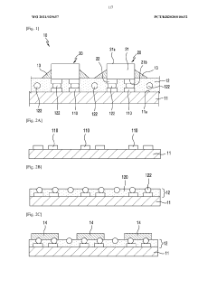
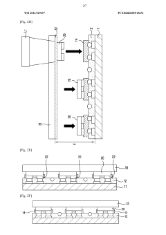
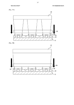
Micro LED display and manufacturing method thereof
PatentWO2021029657A1
Innovation
- The use of an anisotropic conductive film with conductive particles for electrically and physically connecting micro LED chips to a substrate, involving bonding, laser transfer, and heating to form a conductive structure between the chip's connection pad and the substrate's circuit part.
Supply Chain Considerations and Material Sourcing Challenges
The supply chain for OLED and MicroLED technologies presents distinct challenges that significantly impact mass production capabilities. For OLED manufacturing, the supply chain heavily depends on specialized organic materials that are predominantly controlled by a limited number of suppliers, primarily from South Korea and Japan. This concentration creates vulnerability to supply disruptions and price fluctuations, particularly affecting smaller manufacturers without established supplier relationships.
Material sourcing for OLED production involves complex organic compounds that require stringent purity standards exceeding 99.99%. These materials often have limited shelf life and require specialized handling and storage conditions, adding logistical complexity to the supply chain. Additionally, the rare metals used in OLED production, such as indium, face potential supply constraints as global demand increases across multiple industries.
MicroLED technology encounters different but equally challenging supply chain issues. The production requires specialized epitaxial wafers, typically gallium nitride (GaN) grown on sapphire or silicon carbide substrates. These materials face production capacity limitations and quality consistency challenges across suppliers. The mass transfer equipment needed for MicroLED assembly represents another critical supply chain bottleneck, with only a handful of equipment manufacturers capable of producing the precision machinery required.
Both technologies face geopolitical risks in their supply chains. OLED material production is concentrated in East Asia, while MicroLED depends on semiconductor manufacturing capabilities spread across Taiwan, Japan, and the United States. Trade tensions and regional conflicts could significantly disrupt material availability and increase production costs for both technologies.
Sustainability considerations are increasingly affecting supply chain strategies. OLED manufacturing uses several rare materials with environmental extraction concerns, while MicroLED production requires energy-intensive processes. As environmental regulations tighten globally, manufacturers must develop more sustainable sourcing practices, potentially restructuring existing supply chains and material sourcing approaches.
The COVID-19 pandemic exposed additional vulnerabilities in these high-tech supply chains, prompting manufacturers to pursue greater diversification of suppliers and increased vertical integration. Companies leading in both technologies are increasingly investing in securing their supply chains through strategic partnerships, long-term contracts, and in some cases, direct investment in material production capabilities to mitigate future disruption risks.
Environmental Impact and Sustainability of Display Manufacturing
The manufacturing processes for both OLED and MicroLED displays present significant environmental challenges that require careful consideration as these technologies scale for mass production. OLED production involves the use of numerous hazardous chemicals, including heavy metals and organic solvents that pose environmental risks if not properly managed. The vacuum deposition processes used in OLED manufacturing are particularly energy-intensive, contributing substantially to the carbon footprint of each display produced.
MicroLED manufacturing, while promising greater energy efficiency in the end product, currently faces its own sustainability challenges. The production process requires rare earth elements for the LED components, raising concerns about resource depletion and the environmental impact of mining operations. Additionally, the transfer process for MicroLED pixels generates considerable material waste, as defective units must be discarded during the precise placement procedures.
Water consumption represents another critical environmental factor in display manufacturing. Both technologies require ultra-pure water for cleaning processes, with a single manufacturing facility potentially consuming millions of gallons daily. OLED facilities typically have higher water usage due to the multiple organic layer deposition steps, while MicroLED production may eventually reduce water requirements as pick-and-place technologies improve.
Energy efficiency during the product lifecycle partially offsets manufacturing impacts. MicroLED displays demonstrate superior energy efficiency during operation compared to OLEDs, potentially reducing their lifetime environmental impact despite more resource-intensive production. However, end-of-life considerations remain problematic for both technologies, as the complex material composition makes recycling challenging.
Several manufacturers have begun implementing sustainability initiatives to address these concerns. These include closed-loop water recycling systems, renewable energy investments for manufacturing facilities, and research into less toxic material alternatives. Samsung and LG have established ambitious carbon neutrality targets for their display divisions, while Apple has committed to using recycled rare earth elements in their future display technologies.
Regulatory frameworks are increasingly influencing manufacturing practices, with the EU's Restriction of Hazardous Substances (RoHS) directive and similar regulations worldwide pushing manufacturers toward greener production methods. As consumer awareness of environmental issues grows, sustainability is becoming a competitive advantage in the display market, driving further innovation in eco-friendly manufacturing processes.
Unlock deeper insights with Patsnap Eureka Quick Research — get a full tech report to explore trends and direct your research. Try now!
Generate Your Research Report Instantly with AI Agent
Supercharge your innovation with Patsnap Eureka AI Agent Platform!