

Why Flexible OLED Encapsulation Requires Advanced Material Science
SEP 28, 20259 MIN READ
Generate Your Research Report Instantly with AI Agent
Patsnap Eureka helps you evaluate technical feasibility & market potential.
Flexible OLED Encapsulation Evolution and Objectives
Flexible OLED (Organic Light Emitting Diode) technology has evolved significantly over the past two decades, transforming from a laboratory curiosity to a commercial reality that powers cutting-edge displays in smartphones, wearables, and other consumer electronics. The journey began in the early 2000s when researchers first demonstrated the feasibility of creating OLEDs on flexible substrates, primarily using plastic materials instead of traditional glass.
The evolution of flexible OLED encapsulation technology can be traced through several distinct phases. Initially, rigid glass encapsulation methods were adapted for flexible applications, but these proved inadequate due to their inherent brittleness. By the mid-2000s, the industry shifted toward thin-film encapsulation (TFE) techniques, which represented a significant breakthrough by eliminating the need for rigid protective layers.
From 2010 to 2015, multilayer barrier films emerged as the dominant approach, alternating organic and inorganic layers to create tortuous paths that prevented moisture and oxygen penetration. This period saw the development of atomic layer deposition (ALD) techniques that enabled the creation of ultra-thin yet highly effective barrier layers, measuring just nanometers in thickness.
The most recent evolutionary phase, from 2016 to present, has focused on hybrid encapsulation solutions that combine multiple technologies to achieve optimal performance. These systems typically incorporate inorganic barrier layers for superior moisture resistance, organic layers for flexibility and stress relief, and edge sealants to prevent lateral ingress of contaminants.
The primary objective of flexible OLED encapsulation research is to develop barrier systems that simultaneously achieve seemingly contradictory properties: exceptional barrier performance against oxygen and moisture (requiring water vapor transmission rates below 10^-6 g/m²/day), mechanical flexibility to withstand repeated bending (over 200,000 cycles at radii below 5mm), optical transparency exceeding 90%, and thinness below 10 micrometers—all while maintaining cost-effectiveness for mass production.
Secondary objectives include extending device lifetimes beyond 10,000 hours under various environmental conditions, reducing production costs to enable broader market adoption, and developing environmentally sustainable encapsulation materials that reduce reliance on rare elements and hazardous chemicals. The ultimate goal is to enable truly foldable and rollable displays that can withstand daily use while maintaining perfect visual performance.
As flexible display applications expand into new territories such as automotive dashboards, medical devices, and architectural elements, encapsulation technology must continue to evolve to meet increasingly demanding requirements for durability, flexibility, and performance in diverse operating environments.
Market Demand Analysis for Flexible Display Technologies
The flexible display market has witnessed exponential growth over the past decade, driven primarily by consumer electronics applications. Market research indicates that the global flexible display market is projected to reach $42 billion by 2025, with a compound annual growth rate (CAGR) of approximately 28% from 2020 to 2025. This remarkable growth trajectory is fueled by increasing consumer demand for innovative form factors in smartphones, wearables, and other portable electronic devices.
Consumer preferences have shifted dramatically toward devices with larger screens that maintain portability, creating a perfect opportunity for flexible OLED technology. Surveys reveal that over 70% of smartphone users consider display quality and design as critical factors in purchasing decisions, with flexibility and durability emerging as key differentiators in premium market segments.
The automotive industry represents another significant growth vector for flexible display technologies. Premium vehicle manufacturers are increasingly incorporating curved and flexible displays in dashboard systems, center consoles, and entertainment units. Industry analysts predict that the automotive flexible display segment will grow at a CAGR of 32% through 2025, outpacing the overall market growth rate.
Healthcare and military applications are emerging as promising niche markets for flexible display technologies. Medical devices with conformable displays enable better patient monitoring and more ergonomic equipment design. Similarly, military applications benefit from rugged, lightweight displays that can withstand harsh environmental conditions while maintaining operational efficiency.
Regional market analysis reveals Asia-Pacific as the dominant manufacturing hub, with South Korea, Japan, and China leading production capacity. However, North America and Europe represent the most lucrative markets in terms of premium pricing and technology adoption, particularly in specialized industrial applications.
The sustainability aspect of flexible displays is increasingly influencing market dynamics. Environmental regulations and consumer awareness are driving demand for more energy-efficient and recyclable display technologies. Manufacturers capable of addressing these concerns through advanced material science innovations in encapsulation and substrate technologies are likely to capture greater market share.
Supply chain challenges remain a significant concern for market expansion. The specialized materials required for flexible OLED encapsulation face production scaling issues, with current global capacity meeting only about 65% of projected demand. This supply-demand gap presents both a challenge and an opportunity for materials science companies focused on developing next-generation encapsulation solutions.
Current Barriers in Flexible OLED Encapsulation Materials
Flexible OLED encapsulation faces significant material science challenges that currently impede widespread commercialization and performance optimization. The primary barrier remains the inherent conflict between flexibility requirements and barrier properties. Traditional rigid glass encapsulation provides excellent moisture and oxygen barrier properties (water vapor transmission rate <10^-6 g/m²/day) but lacks the flexibility needed for bendable displays, creating a fundamental materials science paradox.
Thin-film encapsulation (TFE) technologies, while promising, struggle with maintaining barrier integrity during repeated bending cycles. Current inorganic materials like aluminum oxide and silicon nitride exhibit excellent barrier properties but develop microcracks at bend radii below 5mm, creating permeation pathways for moisture and oxygen that accelerate OLED degradation. These microcracks propagate with repeated flexing, significantly reducing device lifespan in real-world applications.
Organic materials used in hybrid encapsulation schemes offer flexibility but provide insufficient barrier properties alone, with typical water vapor transmission rates orders of magnitude higher than required. The interface between organic and inorganic layers in multilayer structures represents another critical weakness, with delamination occurring during thermal cycling and mechanical stress, compromising the entire barrier system.
Manufacturing scalability presents another significant barrier. Current atomic layer deposition (ALD) processes for high-quality barrier films are time-consuming and expensive, with deposition rates typically below 2nm/minute. This creates a production bottleneck that increases manufacturing costs and limits market penetration of flexible OLED technologies.
Temperature sensitivity of the OLED materials restricts processing options for encapsulation layers. Most high-performance barrier materials require deposition or curing temperatures exceeding 200°C, while OLED organic layers typically degrade above 100-120°C, forcing compromises in barrier quality or requiring complex multi-stage manufacturing processes.
Edge sealing remains particularly problematic for flexible displays. The perimeter of the display represents a vulnerable point where moisture can penetrate laterally, bypassing the primary encapsulation layers. Current edge sealing materials lack the combination of flexibility, adhesion strength, and barrier properties needed for reliable long-term protection.
Transparency requirements further constrain material selection, as encapsulation layers must maintain >90% optical transparency across the visible spectrum while providing barrier functionality. Many high-performance barrier materials impart color shifts or reduce light output, directly impacting display quality and energy efficiency.
Contemporary Encapsulation Architectures and Methodologies
01 Multilayer encapsulation structures for flexible OLEDs
Multilayer encapsulation structures are used to enhance the flexibility of OLED devices while maintaining effective barrier properties against moisture and oxygen. These structures typically consist of alternating inorganic and organic layers, where the inorganic layers provide barrier properties and the organic layers provide flexibility and stress relief. The combination allows the encapsulation to bend without cracking while maintaining protection for the sensitive OLED components.- Multilayer encapsulation structures for flexible OLEDs: Multilayer encapsulation structures combine inorganic barrier layers with organic buffer layers to provide both effective moisture/oxygen protection and mechanical flexibility. The inorganic layers (such as silicon nitride, aluminum oxide) provide barrier properties while the organic layers (such as polymers) accommodate bending stress. This alternating structure prevents crack propagation through the entire encapsulation, maintaining barrier properties even when flexed.
- Thin-film encapsulation techniques for flexibility: Thin-film encapsulation (TFE) techniques deposit ultra-thin barrier layers directly onto OLED devices, eliminating the need for rigid glass encapsulation. These techniques include atomic layer deposition (ALD), plasma-enhanced chemical vapor deposition (PECVD), and other vacuum deposition methods that create conformal, pinhole-free barriers while maintaining the overall thinness required for flexibility. The reduced thickness compared to traditional encapsulation significantly improves bending radius capabilities.
- Stress-relief patterns and structures in encapsulation layers: Incorporating specific patterns, structures, or geometrical features into encapsulation layers helps relieve mechanical stress during bending. These include micro-patterns, mesh structures, island-bridge configurations, or strategically placed stress-relief cuts that allow the encapsulation to flex without cracking. Some designs incorporate stretchable interconnects between more rigid encapsulation segments to accommodate bending while maintaining barrier properties.
- Flexible inorganic-organic hybrid materials: Novel hybrid materials combine the barrier properties of inorganic materials with the flexibility of organic compounds. These include organosilicon compounds, metal-organic frameworks, hybrid nanocomposites, and polymer-ceramic hybrids. The molecular-level integration of organic and inorganic components creates materials that maintain excellent barrier properties while exhibiting inherent flexibility, eliminating the sharp interfaces that typically lead to cracking in traditional multilayer structures.
- Edge sealing and mechanical decoupling techniques: Special attention to edge sealing and mechanical decoupling between layers enhances overall flexibility. Edge sealing techniques prevent moisture ingress at the vulnerable perimeter of devices, using flexible sealants or specialized edge structures. Mechanical decoupling approaches use intermediate layers with carefully engineered adhesion properties to prevent stress transfer between layers. Some designs incorporate floating or partially attached structures that can move independently during bending.
02 Thin film encapsulation techniques for flexibility
Thin film encapsulation (TFE) techniques are employed to create ultra-thin barrier layers that can withstand bending and folding while protecting OLED devices. These techniques involve depositing thin layers of materials such as silicon nitride, aluminum oxide, or hybrid materials directly onto the OLED structure. The reduced thickness of these encapsulation layers compared to traditional methods allows for greater flexibility while maintaining barrier performance against environmental contaminants.Expand Specific Solutions03 Stress-relieving structures in encapsulation layers
Various stress-relieving structures are incorporated into OLED encapsulation layers to improve flexibility and prevent cracking during bending. These include micro-patterns, grid structures, or engineered interfaces between different materials that can absorb mechanical stress. Some designs incorporate buffer layers or elastomeric materials that can deform without compromising the barrier properties, allowing the OLED device to flex repeatedly without degradation.Expand Specific Solutions04 Advanced barrier materials for flexible encapsulation
Novel materials are developed specifically for flexible OLED encapsulation, combining high barrier properties with mechanical flexibility. These include hybrid organic-inorganic composites, nanocomposite materials, and specially formulated polymers with enhanced barrier properties. Some approaches use materials that can self-heal minor defects that occur during bending, ensuring long-term protection even under repeated flexing conditions.Expand Specific Solutions05 Edge sealing techniques for flexible OLEDs
Specialized edge sealing methods are employed to prevent moisture and oxygen ingress at the vulnerable edges of flexible OLED displays. These techniques include advanced adhesives, laser sealing processes, or mechanical interlocking structures that maintain their integrity during bending. Some approaches incorporate flexible filler materials or gradient structures at the edges to accommodate the stress concentration that occurs during flexing while maintaining an effective seal around the perimeter of the device.Expand Specific Solutions
Leading Companies in Advanced Encapsulation Solutions
The flexible OLED encapsulation market is currently in a growth phase, with an estimated global market size exceeding $2 billion and projected to expand at a CAGR of 15-20% through 2028. The technology remains in mid-maturity, with significant R&D investments focused on barrier films and advanced materials to prevent moisture and oxygen penetration. Key players like Samsung Display, LG Display, and BOE Technology are leading innovation, while Chinese manufacturers including TCL China Star and Everdisplay Optronics are rapidly advancing their capabilities. Applied Materials and LG Chem provide critical materials and equipment. The competitive landscape shows established Korean companies maintaining technological leadership, though Chinese firms are closing the gap through aggressive investment in manufacturing capacity and proprietary encapsulation solutions.
BOE Technology Group Co., Ltd.
Technical Solution: BOE has developed an innovative flexible OLED encapsulation technology called "Multi-Buffer Encapsulation" (MBE) that addresses the critical challenges of moisture barrier performance and mechanical flexibility. Their approach employs a sophisticated stack of alternating inorganic and organic layers, with the inorganic layers (typically silicon nitride and aluminum oxide) deposited using plasma-enhanced atomic layer deposition (PEALD) at lower temperatures (below 100°C) to prevent thermal damage to the OLED materials. BOE's proprietary organic interlayers utilize specially formulated acrylate polymers with enhanced cross-linking density that provide both stress relief during bending and additional barrier properties. Their technology incorporates "buffer zones" - engineered interfaces between layers that prevent crack propagation and improve adhesion. Recent advancements include the integration of graphene oxide nanosheets into the barrier structure, which has demonstrated a significant improvement in gas barrier properties while maintaining excellent mechanical flexibility. BOE has also developed a unique edge sealing technology using laser-assisted patterning to create seamless encapsulation around display edges.
Strengths: Excellent moisture barrier performance with WVTR below 5×10^-7 g/m²/day; superior mechanical durability allowing for over 200,000 folding cycles; compatibility with various substrate materials. Weaknesses: Higher production costs compared to traditional encapsulation methods; complex multi-step manufacturing process requiring precise control; potential for optical performance degradation due to multiple layer interfaces.
Applied Materials, Inc.
Technical Solution: Applied Materials has developed a comprehensive flexible OLED encapsulation solution called "Barrier Film Technology Platform" that addresses the fundamental challenges of protecting flexible displays from moisture and oxygen while maintaining mechanical flexibility. Their approach utilizes a proprietary roll-to-roll vacuum deposition system that can create ultra-thin barrier films with precisely controlled thickness and composition. The technology employs a multi-layer architecture consisting of alternating inorganic barrier layers (primarily aluminum oxide and silicon nitride) deposited via plasma-enhanced chemical vapor deposition (PECVD) and organic smoothing layers applied through specialized polymer deposition techniques. Applied Materials' system can achieve inorganic layer thicknesses below 20nm with exceptional uniformity across large substrates, which is critical for maintaining barrier performance during bending. Their latest innovation incorporates nanolaminate structures with dozens of ultra-thin alternating layers that significantly reduce the permeation path for water molecules while distributing mechanical stress during flexing. The company has also developed advanced in-line metrology tools that can detect nano-scale defects in barrier films during production, enabling real-time process optimization and quality control.
Strengths: Industry-leading barrier film uniformity and defect control; scalable manufacturing technology suitable for high-volume production; comprehensive materials science approach addressing both barrier performance and mechanical requirements. Weaknesses: Capital-intensive equipment requirements; complex process integration challenges when implementing in existing manufacturing lines; ongoing optimization needed for different display configurations and bending requirements.
Breakthrough Materials Science Innovations for Flexible OLEDs
Flexible organic light-emitting diode (OLED) device and fabrication method thereof
PatentActiveUS20210336206A1
Innovation
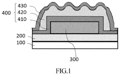
- A novel encapsulation layer configuration with a first and second inorganic layer and an organic layer, where the second inorganic layer has a continuous wavy curved configuration, increasing contact area and reducing stress, formed spontaneously due to thermal stress differences between layers.
Organic light-emitting diode (OLED) encapsulation methods and OLED encapsulation structure
PatentActiveUS20180233700A1
Innovation
- An OLED encapsulation method combining frame glue and thin film encapsulation technologies, where frame glue limits the organic layer's dimension, allowing complete coverage by inorganic layers, and using silicon oxide, silicon nitride, or aluminum oxide layers deposited by PECVD, ALD, or sputtering to enhance encapsulation and reduce manufacturing complexity.


Environmental Impact of Encapsulation Materials
The environmental implications of encapsulation materials used in flexible OLED technology represent a growing concern as production volumes increase globally. Traditional encapsulation approaches often rely on materials with significant ecological footprints, including rare earth elements, heavy metals, and petroleum-based polymers that pose end-of-life disposal challenges.
Thin-film barrier materials commonly used in OLED encapsulation, particularly aluminum oxide and silicon nitride, require energy-intensive deposition processes that contribute to carbon emissions. The vacuum deposition techniques employed in manufacturing these barriers consume substantial electricity, with estimates suggesting that encapsulation processes may account for 15-20% of the total energy consumption in OLED production.
Chemical waste generation presents another environmental challenge. The etching and cleaning processes associated with encapsulation layer deposition produce hazardous byproducts including perfluorinated compounds and various solvents that require specialized disposal protocols. Many of these chemicals have high global warming potentials and long atmospheric lifetimes.
Emerging bio-based alternatives show promise for reducing environmental impact. Research into cellulose-derived barrier films and plant-based adhesives demonstrates potential pathways toward more sustainable encapsulation solutions. These materials offer biodegradability advantages while maintaining acceptable barrier properties, though their moisture sensitivity remains a limitation requiring additional protective measures.
Recycling challenges are particularly acute for flexible OLED devices. The multi-layer structure of encapsulation systems creates separation difficulties at end-of-life, often rendering the materials non-recoverable through conventional recycling streams. This contributes to electronic waste accumulation, with flexible display components increasingly entering the waste stream as consumer electronics adoption grows.
Life cycle assessment studies indicate that transitioning to water-based adhesives and reducing halogenated compounds in encapsulation layers could decrease the environmental footprint by 30-40% compared to conventional approaches. Several major display manufacturers have initiated programs to develop encapsulation technologies with reduced environmental impact, recognizing both regulatory pressure and market demand for greener electronics.
The development of solvent-free deposition techniques represents another promising direction for environmental improvement. Atomic layer deposition methods that minimize chemical waste while maintaining high-quality barrier properties are gaining traction, though scaling challenges remain for high-volume manufacturing implementation.
Scalability Challenges in Advanced Material Manufacturing
The manufacturing of advanced materials for flexible OLED encapsulation faces significant scalability challenges that currently impede widespread commercial adoption. Traditional manufacturing processes designed for rigid displays cannot be directly transferred to flexible OLED production, creating a fundamental bottleneck in the industry's growth trajectory.
Material consistency represents one of the most pressing challenges. When scaling from laboratory prototypes to mass production, maintaining uniform barrier properties across large substrate areas becomes increasingly difficult. Even minor variations in thin film deposition can create weak points in the encapsulation layer, leading to moisture ingress and premature device failure. This challenge is particularly acute for multi-layer barrier systems where defect alignment across layers must be carefully controlled.
Equipment limitations further compound these issues. Current vapor deposition systems struggle to achieve the necessary precision at high throughput rates required for commercial viability. The capital expenditure for specialized equipment capable of handling flexible substrates at scale remains prohibitively high for many manufacturers, creating market entry barriers and limiting competition.
Process integration presents another significant hurdle. Advanced encapsulation materials must be compatible with existing manufacturing workflows, including pre-deposition surface treatments and post-deposition processing. The thermal budget constraints of flexible substrates (typically limited to 100-150°C) severely restrict the available processing window, eliminating many conventional approaches that require high-temperature annealing.
Yield management becomes exponentially more complex at scale. The detection of nanoscale defects in barrier layers across large-area substrates requires sophisticated in-line monitoring systems that do not currently exist in production environments. Without adequate quality control mechanisms, manufacturers face unacceptable rejection rates that undermine economic feasibility.
Supply chain considerations also impact scalability. Many advanced barrier materials rely on rare elements or proprietary formulations with limited supplier networks. This creates potential bottlenecks in material availability and price volatility that can disrupt production planning. The environmental impact of these specialized materials must also be addressed, as regulatory requirements increasingly demand sustainable manufacturing practices.
Addressing these scalability challenges requires coordinated efforts across material science, equipment engineering, and process development. Recent innovations in atomic layer deposition (ALD) and solution-processed barrier materials show promise for overcoming some of these limitations, but significant investment in manufacturing infrastructure remains necessary before flexible OLED encapsulation can achieve the cost structure needed for mass-market adoption.
Unlock deeper insights with Patsnap Eureka Quick Research — get a full tech report to explore trends and direct your research. Try now!
Generate Your Research Report Instantly with AI Agent
Supercharge your innovation with Patsnap Eureka AI Agent Platform!