Why Resistive RAM Advances Are Crucial for Future Electronics
OCT 9, 20259 MIN READ
Generate Your Research Report Instantly with AI Agent
Patsnap Eureka helps you evaluate technical feasibility & market potential.
ReRAM Technology Background and Objectives
Resistive Random Access Memory (ReRAM) represents a revolutionary advancement in non-volatile memory technology, emerging as a promising solution to address the growing limitations of conventional memory systems. The evolution of ReRAM can be traced back to the early 2000s when researchers began exploring alternative memory technologies to overcome the scaling challenges faced by traditional Flash memory. Since then, ReRAM has undergone significant development, transitioning from a theoretical concept to practical implementations with commercial potential.
The fundamental operating principle of ReRAM is based on the reversible change in resistance of a dielectric material, typically a metal oxide, when subjected to an electric field. This resistance switching mechanism enables the storage of binary information, with high and low resistance states representing the '0' and '1' bits. The simplicity of this mechanism, combined with its compatibility with conventional CMOS fabrication processes, has positioned ReRAM as a viable candidate for next-generation memory solutions.
The technological trajectory of ReRAM has been characterized by continuous improvements in performance metrics, including switching speed, endurance, retention time, and power consumption. Early ReRAM devices suffered from reliability issues and limited endurance, but recent advancements have significantly enhanced these parameters, bringing them closer to the requirements for mainstream adoption. The development of novel materials, device architectures, and fabrication techniques has been instrumental in driving this progress.
The primary objective of ReRAM technology is to address the growing gap between processing capabilities and memory performance in modern computing systems, often referred to as the "memory wall." As data-intensive applications become increasingly prevalent, the demand for high-speed, energy-efficient, and scalable memory solutions has intensified. ReRAM aims to fulfill this demand by offering superior performance characteristics compared to existing technologies.
Beyond conventional computing applications, ReRAM holds significant promise for emerging domains such as neuromorphic computing, edge AI, and Internet of Things (IoT) devices. Its ability to mimic synaptic behavior makes it particularly suitable for implementing artificial neural networks in hardware, potentially enabling more efficient and powerful AI systems. Additionally, the low power consumption and non-volatility of ReRAM make it ideal for energy-constrained IoT applications.
Looking ahead, the evolution of ReRAM technology is expected to continue along multiple fronts, including material optimization, device scaling, and integration with advanced computing architectures. The ultimate goal is to establish ReRAM as a universal memory solution that combines the speed of SRAM, the density of DRAM, and the non-volatility of Flash memory, thereby revolutionizing the memory hierarchy in future electronic systems.
Market Demand Analysis for Next-Generation Memory
The global memory market is experiencing a significant shift driven by the increasing demands of emerging technologies such as artificial intelligence, Internet of Things (IoT), autonomous vehicles, and 5G networks. These applications require memory solutions that offer higher density, lower power consumption, faster speeds, and non-volatility – characteristics that traditional memory technologies struggle to deliver simultaneously. This market evolution has created substantial opportunities for next-generation memory technologies, particularly Resistive RAM (ReRAM).
Market research indicates that the next-generation memory market is projected to grow at a compound annual growth rate of 26.3% between 2021 and 2026, reaching approximately $13.7 billion by 2026. This growth is primarily fueled by the exponential increase in data generation and processing requirements across various sectors. The traditional memory hierarchy, dominated by DRAM and NAND flash, is increasingly unable to meet these evolving demands, creating a significant market gap for innovative memory solutions.
Consumer electronics remains the largest application segment for next-generation memory technologies, accounting for nearly 40% of the market share. However, enterprise storage systems and automotive applications are emerging as rapidly growing segments, with projected growth rates exceeding 30% annually. This diversification of application areas demonstrates the broad market potential for ReRAM technology.
The demand for energy-efficient computing solutions is another critical market driver. With data centers now consuming more than 2% of global electricity and mobile device manufacturers prioritizing battery life, memory technologies that offer substantial power savings have become increasingly valuable. ReRAM's low power consumption characteristics position it favorably in this market context, with potential power savings of up to 90% compared to conventional memory technologies in certain applications.
Geographically, North America and Asia-Pacific represent the largest markets for next-generation memory technologies, collectively accounting for over 70% of global demand. China's ambitious semiconductor self-sufficiency initiatives and substantial investments in memory technology development have created a particularly dynamic market environment in the Asia-Pacific region.
Industry surveys reveal that system designers across multiple sectors are actively seeking memory solutions that can overcome the "memory wall" – the growing disparity between processing speeds and memory access times. This technical challenge has created market demand for memory architectures that can provide higher bandwidth and lower latency, areas where ReRAM shows significant promise with demonstrated read latencies below 10 nanoseconds in research prototypes.
ReRAM Development Status and Technical Barriers
Resistive RAM (ReRAM) technology has reached a critical development stage with significant advancements in recent years, yet still faces substantial technical barriers that impede widespread commercial adoption. Current ReRAM devices demonstrate promising characteristics including low power consumption, high switching speed, and excellent scalability compared to conventional memory technologies. Leading research institutions and semiconductor companies have achieved ReRAM cells with switching speeds below 10ns and endurance cycles exceeding 10^9, positioning ReRAM as a viable candidate for next-generation non-volatile memory applications.
Despite these achievements, several technical challenges persist in ReRAM development. The most significant barrier remains the variability issue, where device-to-device and cycle-to-cycle variations in resistance states lead to reliability concerns. This variability stems from the stochastic nature of filament formation and rupture processes in oxide-based ReRAM, creating inconsistent switching behaviors that complicate large-array implementation.
Endurance limitations represent another critical barrier, particularly for applications requiring frequent write operations. While some laboratory demonstrations have achieved impressive endurance figures, commercial-grade ReRAM still struggles to maintain consistent performance beyond 10^6-10^7 cycles without degradation, falling short of requirements for universal memory applications that demand 10^12-10^15 cycles.
The retention-versus-switching speed trade-off presents a fundamental challenge in ReRAM design. Devices optimized for long retention times typically require higher operating voltages and exhibit slower switching speeds, while faster devices often sacrifice data retention capability. This inherent conflict complicates ReRAM's positioning in the memory hierarchy.
Material engineering challenges further complicate ReRAM development. The selection and optimization of switching materials, electrode compositions, and interface engineering remain active research areas. Current materials systems often involve complex trade-offs between performance parameters, with no single material combination satisfying all requirements simultaneously.
Integration with CMOS technology presents additional hurdles, particularly regarding process compatibility and thermal budget constraints. The development of selector devices for crossbar arrays to mitigate sneak path currents remains challenging, especially as cell dimensions shrink below 10nm. Current selector technologies often introduce additional resistance or capacitance that degrades overall array performance.
Scaling issues become increasingly prominent as the industry pushes toward higher density memory. At sub-10nm dimensions, quantum effects and material property variations significantly impact device performance and reliability. The physics of filament formation at these scales is not fully understood, creating uncertainty in ultra-scaled ReRAM behavior.
Current ReRAM Implementation Approaches
01 Resistive RAM device structures
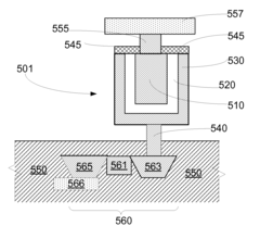
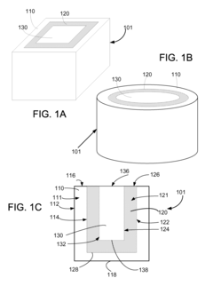
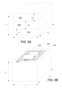
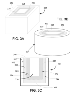
Resistive RAM (RRAM) devices are constructed with specific structures to enable resistive switching behavior. These structures typically include a resistive switching layer sandwiched between two electrodes. Various materials can be used for the resistive switching layer, including metal oxides, chalcogenides, and perovskites. The electrode materials and their interfaces with the switching layer play crucial roles in determining the device performance, including switching speed, endurance, and retention time.- Structure and fabrication of resistive RAM devices: Resistive RAM (RRAM) devices are typically fabricated with a structure consisting of a resistive switching material sandwiched between two electrodes. The resistive switching material can be a metal oxide, chalcogenide, or other materials that exhibit resistive switching behavior. Various fabrication techniques are employed to create these structures, including deposition methods like sputtering, atomic layer deposition, and chemical vapor deposition. The electrode materials and their interfaces with the switching layer play crucial roles in determining the performance characteristics of the RRAM device.
- Resistive switching mechanisms and materials: The resistive switching phenomenon in RRAM devices can occur through various mechanisms, including filamentary conduction, interface-type switching, and phase change. Different materials exhibit different switching behaviors, with metal oxides like HfOx, TaOx, and TiOx being commonly used. Chalcogenide materials are also employed in some RRAM designs. The choice of switching material affects key performance parameters such as switching speed, endurance, retention time, and power consumption. Understanding these mechanisms is crucial for optimizing RRAM device performance.
- Integration and scaling of RRAM technology: Integration of RRAM into existing semiconductor manufacturing processes presents both challenges and opportunities. RRAM devices can be integrated into crossbar arrays to achieve high density memory structures. The scaling potential of RRAM technology allows for continued miniaturization while maintaining performance characteristics. Various approaches to 3D integration have been developed to further increase storage density. Compatibility with CMOS processes is a key consideration for commercial viability, with back-end-of-line integration being a common approach.
- Circuit design and operation for RRAM systems: Specialized circuit designs are required for effective operation of RRAM devices in memory systems. These include sense amplifiers for reading the resistance state, write drivers for programming operations, and address decoders for cell selection. Pulse shaping techniques are employed to optimize the set and reset operations while minimizing power consumption. Various schemes have been developed to address issues like sneak path currents in crossbar arrays. The peripheral circuitry must be designed to accommodate the unique electrical characteristics of RRAM devices, including their non-linear current-voltage behavior.
- Reliability and performance enhancement techniques: Improving the reliability and performance of RRAM devices involves addressing challenges such as variability in switching behavior, endurance limitations, and retention issues. Various techniques have been developed, including doping of the switching layer, engineering of the electrode-oxide interfaces, and optimization of programming algorithms. Multi-level cell operation, where more than two resistance states are utilized in a single cell, can increase storage density but requires careful control of the resistance distribution. Advanced error correction schemes and redundancy approaches are also employed to enhance system-level reliability.
02 Resistive switching mechanisms
The operation of resistive RAM relies on different switching mechanisms that change the resistance state of the device. These mechanisms include filamentary conduction, where conductive filaments form and rupture within the switching layer, and interface-type switching, where the resistance change occurs at the interface between the electrode and the switching layer. The switching can be unipolar or bipolar, depending on whether the same or opposite voltage polarities are required for SET and RESET operations. Understanding these mechanisms is essential for optimizing device performance and reliability.Expand Specific Solutions03 Fabrication methods for Resistive RAM
Various fabrication techniques are employed to manufacture resistive RAM devices with desired characteristics. These include physical vapor deposition (PVD), atomic layer deposition (ALD), chemical vapor deposition (CVD), and solution-based methods. Post-deposition treatments such as annealing and plasma treatments are often used to optimize the properties of the resistive switching layer. Integration with CMOS technology requires careful consideration of process compatibility and thermal budget constraints. Advanced patterning techniques enable the fabrication of high-density RRAM arrays.Expand Specific Solutions04 Circuit design and integration for Resistive RAM
Effective implementation of resistive RAM requires specialized circuit designs for read, write, and erase operations. These circuits must address challenges such as sneak path currents in crossbar arrays, variability in switching behavior, and the need for precise current or voltage control. Integration approaches include 1T1R (one transistor, one resistor) and crossbar architectures. Peripheral circuits for sensing, addressing, and programming are critical for reliable operation. Advanced designs incorporate features for error correction, wear leveling, and adaptive programming to enhance endurance and reliability.Expand Specific Solutions05 Applications and emerging technologies for Resistive RAM
Resistive RAM finds applications in non-volatile memory, neuromorphic computing, and in-memory computing. In neuromorphic applications, RRAM devices can mimic synaptic behavior, enabling efficient implementation of artificial neural networks. For storage applications, RRAM offers advantages such as high density, low power consumption, and fast switching speed. Emerging technologies include multi-level cell operation, where multiple resistance states are used to store more than one bit per cell, and 3D integration for ultra-high density storage. Research is also exploring the use of novel materials and device structures to further enhance performance and functionality.Expand Specific Solutions
Key Industry Players in ReRAM Development
Resistive RAM (ReRAM) technology is currently in the early growth phase of its industry lifecycle, with significant potential to revolutionize future electronics. The global ReRAM market is projected to expand rapidly, driven by increasing demand for high-performance, low-power memory solutions in IoT, AI, and edge computing applications. Leading semiconductor manufacturers including Samsung Electronics, SK hynix, Micron Technology, and TSMC are actively developing ReRAM technologies, while specialized players like CrossBar and Adesto Technologies are pushing innovation boundaries. Research institutions such as Peking University, Nanyang Technological University, and the Institute of Microelectronics of Chinese Academy of Sciences are contributing fundamental breakthroughs. Though still maturing compared to established memory technologies, ReRAM's unique characteristics of non-volatility, high density, and low power consumption position it as a critical advancement for next-generation electronics systems.
Micron Technology, Inc.
Technical Solution: Micron has developed a comprehensive Resistive RAM technology platform based on their 3D XPoint architecture (originally co-developed with Intel). Their approach utilizes chalcogenide-based materials with a unique selector device that enables high-density crossbar arrays without sneak path issues. Micron's ReRAM technology demonstrates read latencies of approximately 100ns, write latencies of 500ns-1μs, and endurance ratings of 10^7-10^9 cycles. The company has successfully manufactured ReRAM at the 20nm node and has been working on scaling to more advanced nodes. Micron's technology offers non-volatility with 10+ year retention and operates with significantly lower write energy compared to NAND flash. They have positioned their ReRAM as a storage-class memory bridging the gap between DRAM and NAND flash.
Strengths: Established manufacturing capabilities; experience with 3D XPoint architecture; strong system-level integration expertise. Weaknesses: Strategic pivot away from 3D XPoint; challenges in achieving cost parity with NAND flash; competition from other emerging memory technologies in Micron's portfolio.
International Business Machines Corp.
Technical Solution: IBM has pioneered Phase Change Memory (PCM) technology, a specific type of Resistive RAM that leverages chalcogenide materials (typically Ge2Sb2Te5) that change resistance states based on crystalline structure transitions. IBM's PCM technology achieves multi-level cell capability with 3+ bits per cell, read/write latencies in the 10-100ns range, and endurance exceeding 10^6 cycles. The company has demonstrated working arrays at 14nm with a clear path to sub-10nm nodes. IBM has integrated their PCM technology with their neuromorphic computing platforms, demonstrating analog AI acceleration capabilities. Their approach includes proprietary selector devices that enable high-density crossbar arrays while minimizing sneak path issues. IBM has also explored PCM for in-memory computing applications to overcome the von Neumann bottleneck.
Strengths: Deep research expertise in materials science; strong integration with AI/cognitive computing platforms; advanced selector technology. Weaknesses: Limited manufacturing capabilities compared to memory specialists; primarily focused on research rather than commercial production; complex materials integration challenges.
Critical Patents and Technical Innovations in ReRAM
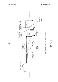
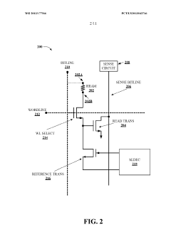
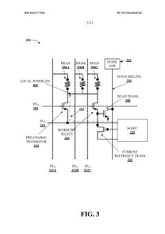
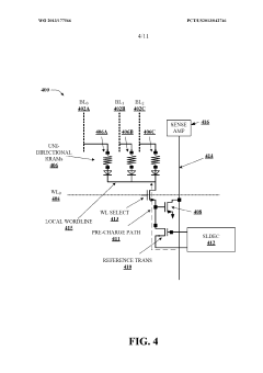
High operating speed resistive random access memory
PatentWO2013177566A1
Innovation
- The development of a high-speed RRAM architecture that connects multiple RRAM devices to a single read transistor, utilizing a reference transistor to apply a bias voltage and mitigate off-current, and employing a sensing circuit to quickly detect changes in electrical characteristics, enabling fast programming, reading, and erasing operations while reducing the number of read transistors and associated circuitry.
Structures for resistive random access memory cells
PatentActiveUS20100110758A1
Innovation
- The RRAM cell design features a trench structure with a first electrode, a resistive layer, and a second electrode that nest inside each other, increasing the contact area between the electrodes and the resistive layer, allowing for larger areal densities and enhanced functioning without increasing the memory chip area.
Energy Efficiency and Sustainability Implications
The energy implications of Resistive RAM (ReRAM) technology represent a critical dimension in evaluating its potential impact on future electronics. Current computing systems based on conventional memory technologies consume substantial amounts of power, contributing significantly to global energy demand. ReRAM offers remarkable advantages in this domain, with power consumption estimates showing potential reductions of 10-100x compared to flash memory and DRAM technologies.
During operation, ReRAM devices require minimal energy to switch between resistance states, typically in the picojoule to femtojoule range per bit operation. This exceptional energy efficiency stems from the fundamental physics of resistive switching mechanisms, which involve localized atomic rearrangements rather than charge movement across large capacitive structures as in conventional memory technologies.
The sustainability benefits extend beyond direct operational energy savings. ReRAM's non-volatile nature eliminates the need for constant power to maintain stored information, addressing a significant source of energy waste in current computing systems. This characteristic is particularly valuable for edge computing devices and IoT applications, where battery life and energy harvesting constraints are paramount considerations.
Manufacturing processes for ReRAM also demonstrate potential environmental advantages. Many ReRAM structures utilize abundant materials like titanium oxide and hafnium oxide, reducing dependence on rare or environmentally problematic elements. The relatively simpler structure of ReRAM cells compared to transistor-based memories may eventually translate to lower manufacturing energy requirements and reduced chemical usage, though comprehensive lifecycle analyses are still emerging.
From a systems perspective, ReRAM enables architectural innovations that further enhance energy efficiency. Near-memory and in-memory computing paradigms facilitated by ReRAM can dramatically reduce the energy-intensive data movement between processing and storage units that dominates power consumption in conventional von Neumann architectures. Studies indicate that such approaches could yield additional order-of-magnitude improvements in computational energy efficiency for specific workloads.
The long-term sustainability implications of widespread ReRAM adoption include potential reductions in electronic waste through increased device longevity and the enablement of more energy-efficient computing paradigms across the technology spectrum. As data centers currently consume approximately 1-2% of global electricity production with projections showing continued growth, ReRAM's energy efficiency characteristics position it as a key technology for sustainable digital infrastructure development.
Integration Challenges with Existing Semiconductor Infrastructure
The integration of Resistive RAM (RRAM) technology into existing semiconductor manufacturing infrastructure presents significant challenges that must be addressed for widespread commercial adoption. Current semiconductor fabrication facilities are optimized for CMOS technology, with established processes, equipment, and materials that have been refined over decades. Introducing RRAM requires substantial modifications to these established workflows, creating technical and economic barriers.
Material compatibility represents a primary integration challenge. RRAM devices typically utilize novel materials such as metal oxides, chalcogenides, or perovskites that are not commonly used in traditional CMOS processes. These materials may introduce contamination risks to existing fabrication lines, potentially compromising the performance of conventional semiconductor devices produced in the same facilities. Specialized handling procedures and dedicated equipment may be necessary, increasing manufacturing complexity and cost.
Process temperature compatibility also presents significant obstacles. Many RRAM fabrication steps require specific thermal budgets that may conflict with established CMOS process flows. High-temperature processes needed for certain RRAM materials can damage previously fabricated CMOS components, while low-temperature requirements for other RRAM structures may limit material quality and device performance. Developing thermally compatible integration schemes remains a critical research focus.
Scaling and uniformity challenges further complicate integration efforts. As device dimensions shrink to meet density requirements for competitive memory solutions, maintaining consistent electrical characteristics across billions of RRAM cells becomes increasingly difficult. Process variations that might be tolerable in larger devices can lead to unacceptable performance disparities at nanoscale dimensions, affecting yield and reliability.
Electrical interfacing between RRAM arrays and CMOS control circuitry introduces additional complexity. Signal integrity, power distribution, and addressing schemes must be carefully designed to maintain RRAM's inherent advantages in speed and energy efficiency. The peripheral circuitry must accommodate the unique electrical characteristics of RRAM cells, including their non-linear switching behavior and variable resistance states.
Economic considerations also impact integration strategies. The semiconductor industry has invested billions in existing infrastructure, creating strong incentives to develop RRAM technologies that leverage these investments rather than requiring entirely new fabrication facilities. This drives research toward "CMOS-compatible" RRAM solutions that can be manufactured using modified versions of existing equipment and processes, even when such approaches may not fully optimize RRAM performance characteristics.
Despite these challenges, significant progress has been made in developing integration pathways for RRAM technology. Back-end-of-line integration approaches, where RRAM elements are fabricated in the metal interconnect layers above CMOS transistors, have shown particular promise for maintaining compatibility with existing manufacturing infrastructure while enabling new memory capabilities.
Unlock deeper insights with Patsnap Eureka Quick Research — get a full tech report to explore trends and direct your research. Try now!
Generate Your Research Report Instantly with AI Agent
Supercharge your innovation with Patsnap Eureka AI Agent Platform!