

Method for preparation of a-b orientated ZnO nanometer linear array
A nanowire array and orientation technology is applied in the field of preparation of ZnO nanowire arrays to achieve the effects of excellent ultraviolet light sensitivity, fast light response speed and high deposition rate
- Summary
- Abstract
- Description
- Claims
- Application Information
AI Technical Summary
Problems solved by technology
Method used
Image

Examples
Embodiment Construction
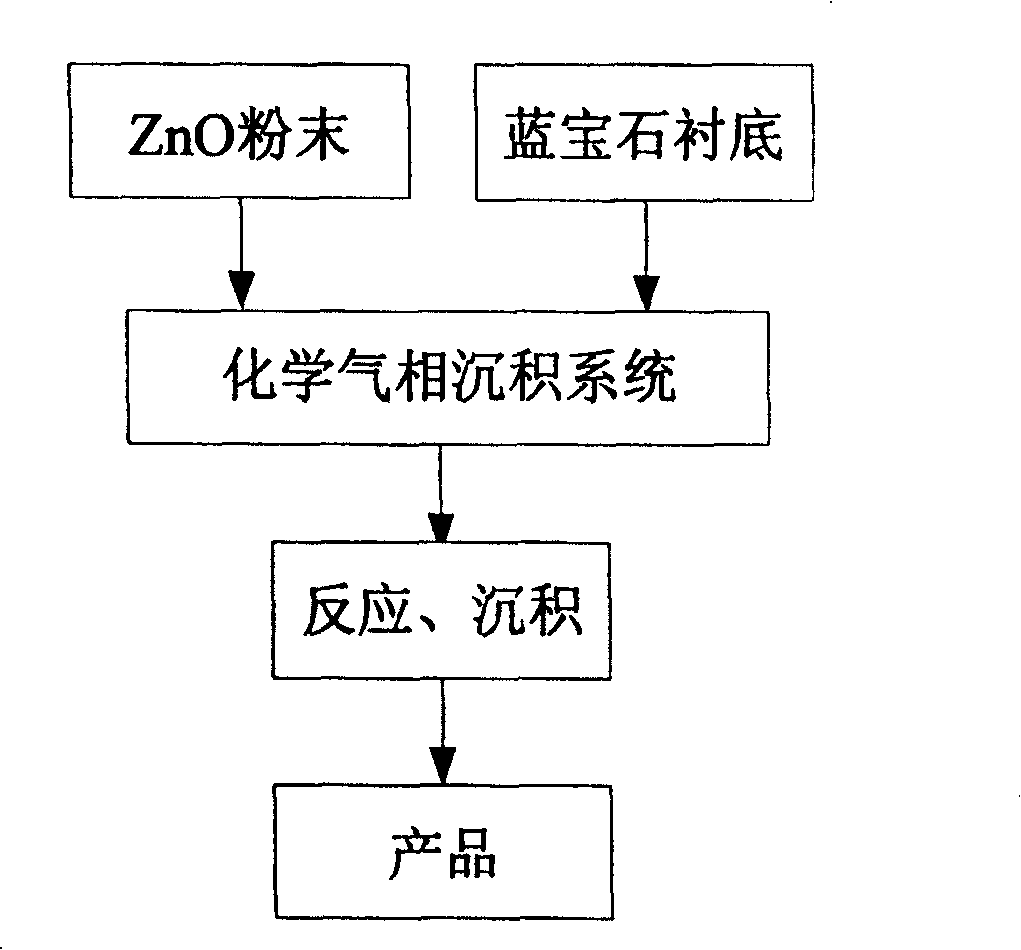
[0026] In the present invention, the ZnO nanowires are prepared by using a dual-temperature zone CVD system. The whole system can be divided into gas circuit part, growth chamber and control part.
[0027] The specific implementation steps are as follows:
[0028] 1. Preparation of Evaporation Source
[0029] In the present invention, analytical pure ZnO powder produced by Tianjin Institute of Chemical Reagents is used as evaporation source.
[0030] 2. Sapphire Al 2 O 3 (1120) cleaning step of substrate substrate:
[0031] 1) scrubbing;
[0032] 2) Soak: use potassium dichromate solution, then wash with deionized water;
[0033] 3) Ultrasonic cleaning 1: deionized water, 5 to 10 minutes, twice;
[0034] 4) Ultrasonic cleaning 2: 5 to 10 minutes in acetone, twice;
[0035] 5) Ultrasonic cleaning 3: in absolute ethanol, 5 to 10 minutes, twice;
[0036] 6) drying;
[0037] 7) Standby.
[0038] 3. CVD synthesis of ZnO nanowires
[0039]Using the high temperature therm...
PUM
| Property | Measurement | Unit |
|---|---|---|
| current | aaaaa | aaaaa |
Abstract
Description
Claims
Application Information