Hardware development platform and hardware development method

A hardware development platform and hardware technology, applied in the direction of printed electrical components, printed circuit parts, multi-core cable end parts, etc., can solve the problems of unbearable financial pressure, non-reusable, inconvenient measurement, etc., to achieve Shorten the hardware development cycle, save development costs, and facilitate debugging

Inactive Publication Date: 2011-02-09
SHANGHAI TOUCHDOWN INFORMATION TECH
View PDF0 Cites 0 Cited by
  • Summary
  • Abstract
  • Description
  • Claims
  • Application Information

AI Technical Summary

Problems solved by technology

[0006] 1. It usually takes 10-20 days to make a PCB, which consumes manpower, material resources and finance
[0007] 2. The cost of PCB production is relatively high, and small and medium-sized companies, especially ordinary electronics enthusiasts and school students, cannot bear the financial pressure
[0008] 3. During the PCB debugging process, because the wiring has been solidified in the PCB board, it is impossible to measure conveniently
[0009] 4. During the PCB debugging process, because the wiring has been solidified in the PCB board, it is impossible to modify the wrong connection conveniently
[0010] 5. If problems are found during PCB debugging, it is generally necessary to redesign the PCB board, and make and debug again
[0011] 6. Ordinary PCB boards are soldered with solder, and ordinary electronics enthusiasts or people other than welders cannot easily modify the wrong connection
[0012] 7. Ordinary PCB boards can only be used once and cannot be reused, resulting in waste

Method used


Image

  • Hardware development platform and hardware development method
  • Hardware development platform and hardware development method
  • Hardware development platform and hardware development method

Examples


Embodiment Construction

[0045] Exemplary embodiments of the present invention are described in detail below, examples of which are illustrated in the accompanying drawings, wherein the same or similar reference numerals refer to the same or similar elements. The embodiments described below with reference to the accompanying drawings are exemplary and intended to explain the present invention, but not to limit the present invention.

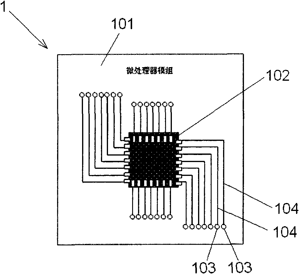
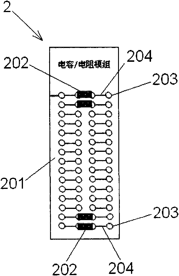
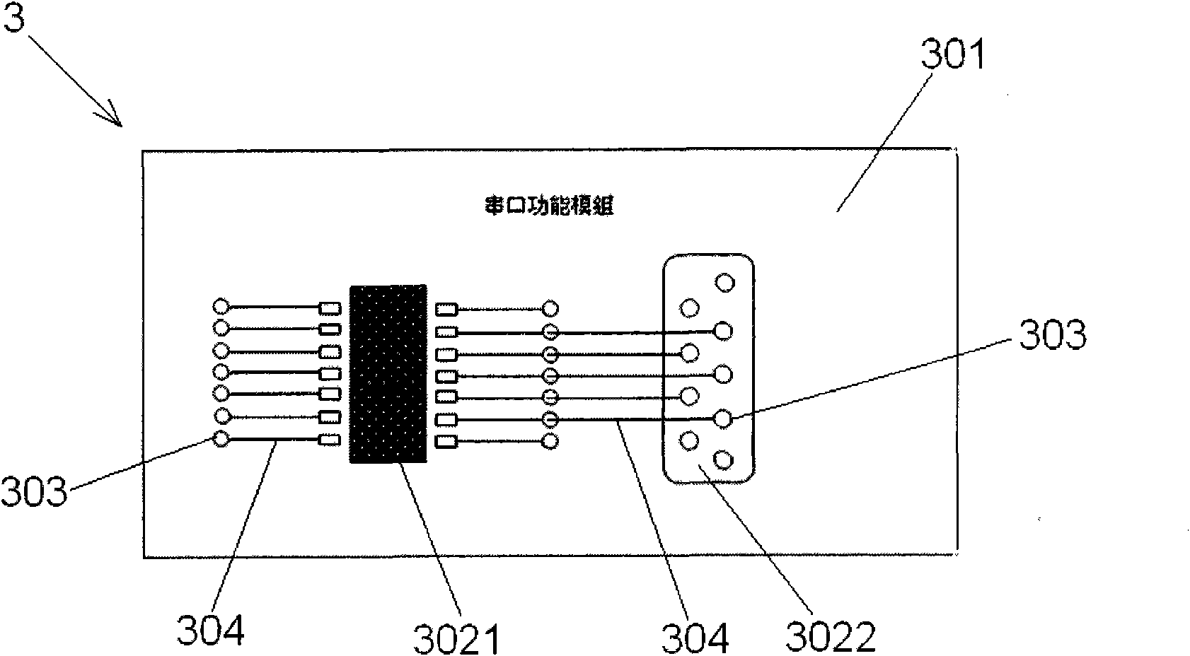
[0046] Figure 1 to Figure 4 A separate function module is displayed respectively. In the present invention, the separate function module is the basic unit that constitutes the hardware development platform (hardware development system) of the present invention, that is, the entire hardware circuit is formed by a plurality of separate function modules. instead of multiple chips and components as in the past.

[0047] specifically, figure 1 A functional module 1 according to an exemplary embodiment of the present invention is shown, and the functional module 1 includes ...


PUM


Abstract

The invention discloses a hardware development platform, which comprises a plurality of functional modules and connecting wires, wherein the connecting wires are used for connecting the plurality of functional modules together; and the connecting wires are connected with the functional modules in a freely-detachable manner. In addition, the invention also provides a hardware development method based on the functional modules. Compared with the prior art, the hardware development platform has the advantages that: due to the free-detachable connection manner of the connecting wires, which are connected between the functional modules, and the functional modules, the connection relationship among functional modules can be changed conveniently for correcting wrong connection in a hardware debugging and test process, so that the debugging is convenient and quick and the remaking process of a board and an entire printed circuit board (PCB) is saved; and thus, the hardware development period is shortened greatly and development cost is saved.

Description

technical field [0001] The invention relates to a hardware development platform and a hardware development method. Background technique [0002] Entering the 21st century, with the rapid development of information technology and electronic technology, the competition in the electronic market is becoming more and more intense. Product quality, product development cycle, and product launch cycle are increasingly being valued by product developers. [0003] All product developers strive to develop products with functions and performance that meet customer needs in the shortest possible time, and to market the products in the shortest time. Otherwise, it may be brutally eliminated by the market. Under this circumstance, how to shorten the product development cycle as soon as possible has become a key consideration for the senior management of each product developer. [0004] In the traditional electronic product design process, PCB design consists of circuit design, PCB layou...

Claims


Application Information

Patent Timeline
Patent Type & Authority Applications(China)
IPC IPC(8): H05K1/11H05K1/16H01R11/11
Inventor 高国明潘建伟
Owner SHANGHAI TOUCHDOWN INFORMATION TECH
Why Eureka
Try Eureka