A low-capacitance multilayer chip varistor and the overvoltage protection layer used therein
An overvoltage and voltage technology, applied in the direction of the varistor core, varistor, etc., can solve the problems of high cost, unfavorable use, and no protection function of the varistor 10
Inactive Publication Date: 2015-09-02
SFI ELECTRONICS TECH
View PDF4 Cites 0 Cited by
- Summary
- Abstract
- Description
- Claims
- Application Information
AI Technical Summary
Problems solved by technology
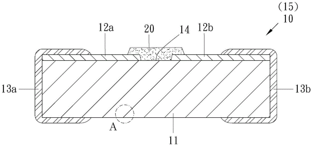
[0007] The disadvantage of this ceramic body 15 is that the ceramic body 11 contains a high content of semiconductor and conductive particles 16. In addition to causing high cost, it is also easy to cause the varistor 10 to generate electricity due to the microporous structure 19. Conduction without protection function, unfavorable for use in high humidity environment
Method used
View moreImage
Smart ImageViewing Examples


Examples
Embodiment 1-3 and comparative example 1-3
[0062] The overvoltage protection material of embodiment 1-3 and comparative example 1-3 is made according to the composition formula of table 1; Figure 4 The gap 34 between the inner electrodes 32a and 32b of the low capacitance varistor 30 of the same specification. Moreover, the structure of the ceramic main body 31 of the low-capacitance varistor 30 has no pores, and completely seals and covers the used overvoltage protection material.
Login to View More PUM
| Property | Measurement | Unit |
|---|---|---|
| particle diameter | aaaaa | aaaaa |
| particle diameter | aaaaa | aaaaa |
Abstract
A low-capacity laminated chip varistor comprises an overvoltage protective material with a special microstructure. The overvoltage protective material contains 10-30 wt% of a porous ceramic substrate, 65-80 wt% of a micron conductor and semiconductor particles and 5-10 wt% of a nano conductor and semiconducting particles. Particularly, the interior of the porous ceramic substrate is provided with micro holes; and the micron conductor and semiconducting particles are uniformly dispersed in the porous ceramic substrate in first grade distribution; and the nano conductor and semiconductive particles are dispersed among the micro holes in second grade distribution, and among the micron conductor and semiconductor nanoparticles in first grade distribution. The special microstructure enables the overvoltage protective material to have the ability to suppress overvoltage and resist 8KV static shock by thousands of times, so the low-capacity laminated chip varistor is suitable for usage in high-humidity environment or / and high-frequency circuit.
Description
technical field [0001] The invention relates to a low-capacity laminated chip varistor, in particular to a low-capacity laminated chip varistor with a capacitance value less than 0.3pF at 1MHz and used for suppressing overvoltage, resisting static shock and protecting electronic circuits. Background technique [0002] Such as figure 1 As shown, a varistor 10 used in a high frequency range includes a ceramic body 11 , a pair of surface electrodes 12 a and 12 b , a pair of end electrodes 13 a and 13 b , and an insulating layer 20 . Wherein, the surface electrodes 12a and 12b are made on the same plane of the outer layer or inner layer of the ceramic body 11 by thin film technology, and the terminal electrodes 13a and 13b are respectively covered on the two ends of the ceramic body 11 , and are respectively electrically connected to the surface electrodes 12a and 12b; moreover, the insulating layer 20 fills the gap 14 between the surface electrodes 12a and 12b. [0003] The i...
Claims
Login to View More Application Information
Patent Timeline
 Patent Type & Authority Patents(China)
IPC IPC(8): H01C7/105
Inventor 连清宏许鸿宗
Owner SFI ELECTRONICS TECH
Features
- R&D
- Intellectual Property
- Life Sciences
- Materials
- Tech Scout
- Unparalleled Data Quality
- Higher Quality Content
- 60% Fewer Hallucinations
Learn More Browse by: Latest US Patents, China's latest patents, Technical Efficacy Thesaurus, Application Domain, Technology Topic, Popular Technical Reports.
© 2025 PatSnap. All rights reserved.Legal|Privacy policy|Modern Slavery Act Transparency Statement|Sitemap|About US| Contact US: help@patsnap.com