Pixel circuit, display panel and display device

A pixel circuit and pixel technology, which is applied in the field of pixel circuits, display panels and display devices, can solve the problems of limited free space of pixel units, restrictions on simultaneous production and space occupation of embedded touch panel circuits, and solve threshold voltage drift , Reduce IC cost and reduce the number of effects

Active Publication Date: 2014-10-01
BOE TECH GRP CO LTD +1
View PDF5 Cites 12 Cited by
  • Summary
  • Abstract
  • Description
  • Claims
  • Application Information

AI Technical Summary

Problems solved by technology

If the TSP sensor and driving circuit are superimposed on the AMOLED pixel, a certain number of driving circuit TFTs need to be added, which requires additional space for a c

Method used


Image

  • Pixel circuit, display panel and display device
  • Pixel circuit, display panel and display device
  • Pixel circuit, display panel and display device

Examples


Embodiment Construction

[0033] The specific implementation manners of the present invention will be further described below in conjunction with the drawings and examples. The following examples are only used to illustrate the technical solution of the present invention more clearly, but not to limit the protection scope of the present invention.

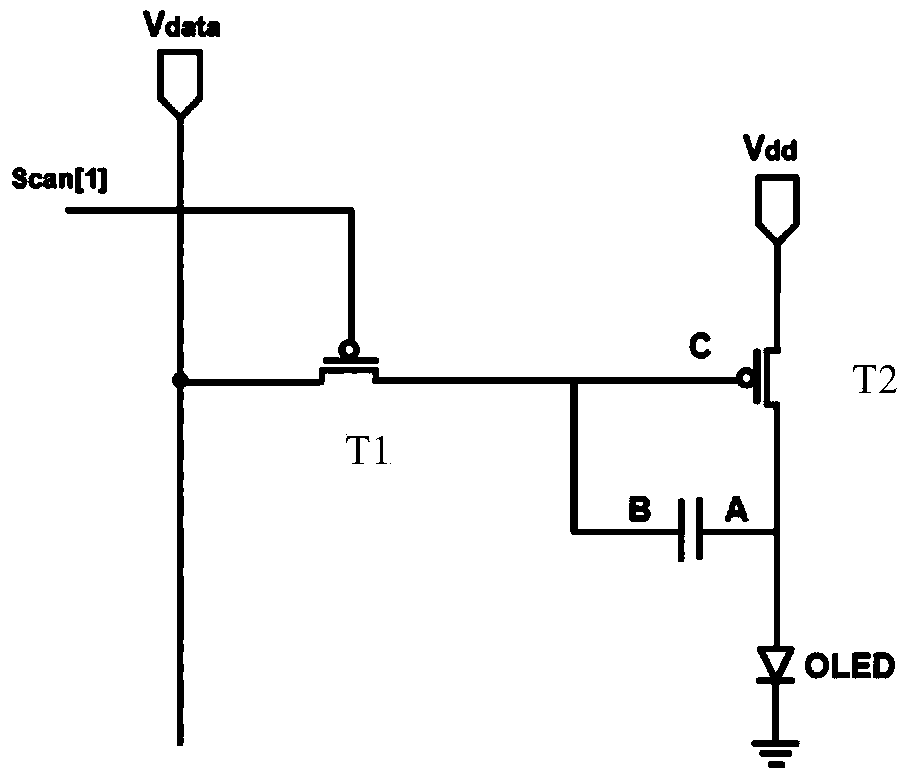
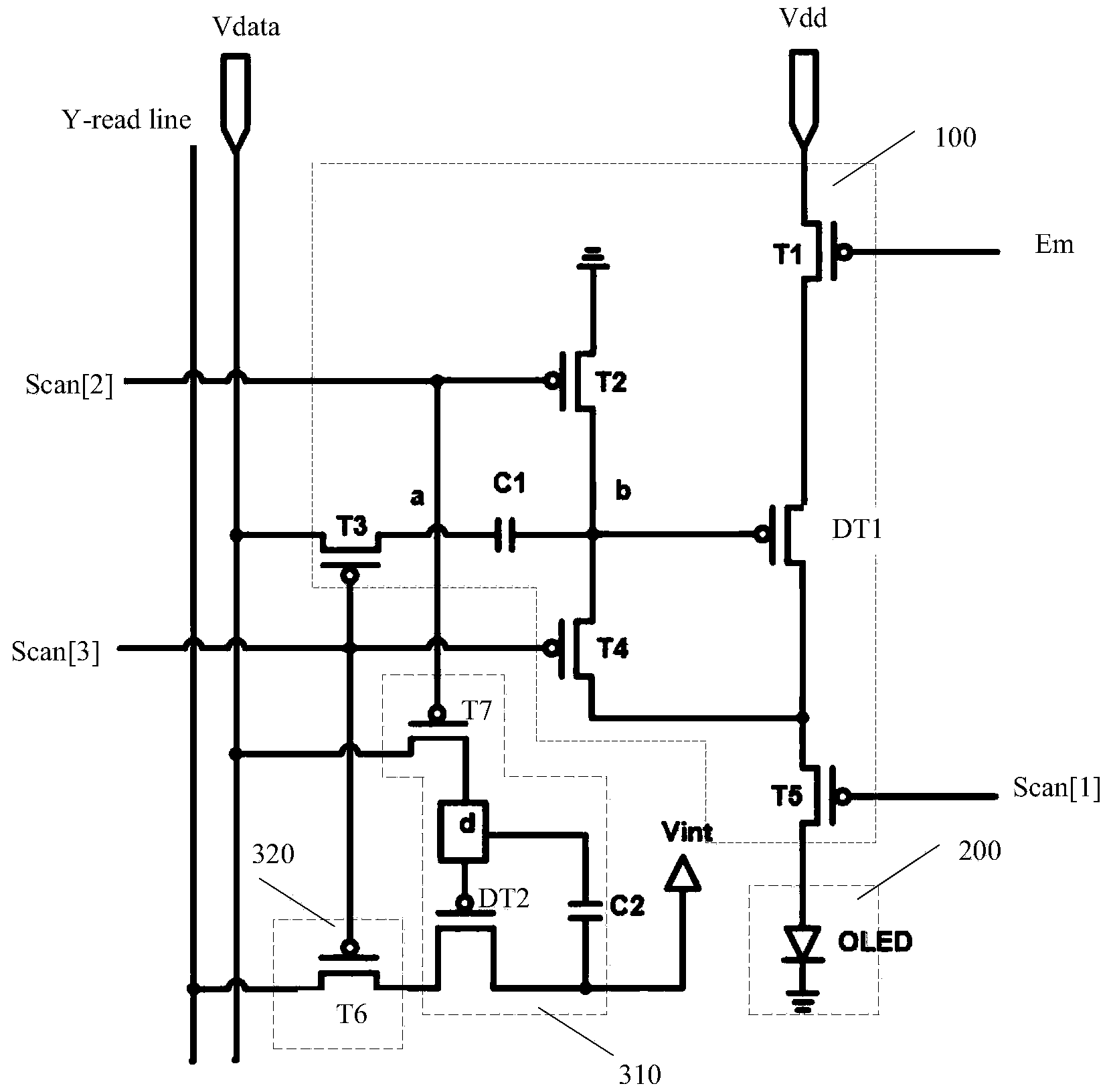
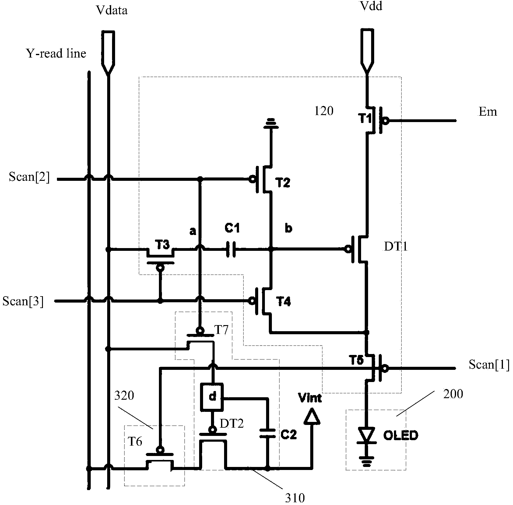
[0034] An embodiment of the present invention provides a pixel circuit, as shown in FIG. 2 , including:

[0035] Pixel compensation module 100, light emitting module 200 and touch detection module;

[0036] Wherein, the pixel compensation module 100 includes a first switching unit T1, a second switching unit T2, a second switching unit T3, a fourth switching unit T4, a fifth switching unit T5, a pixel driving unit DT1, and an energy storage unit C1, wherein,

[0037] The first end of the first switch unit T1 is connected to the first working voltage line Vdd, the second end is connected to the input end of the driving unit DT1, and the control end is conne...


PUM


Abstract

The invention provides a pixel circuit, a display panel and a display device. The pixel circuit comprises a pixel compensating module, a light-emitting module and a touch control detecting module. According to the pixel circuit, the pixel compensating module and the touch control detecting module are integrated, and the pixel compensating module and the touch control detecting module share a data voltage line and a scanning signal line. Thus, the number of signal lines is reduced, the distance between pixels is remarkably reduced, the IC cost is reduced, and the higher pixel density can be achieved. Meanwhile, work current, flowing through an electroluminescent unit, in the pixel circuit cannot be affected by threshold voltage of a corresponding driving transistor. Thus, the problem of uneven display brightness caused by threshold voltage drift of the driving transistor is solved.

Description

technical field [0001] The present invention relates to the field of display technology, in particular to a pixel circuit, a display panel and a display device. Background technique [0002] With the rapid progress of display technology, display devices with touch function are gradually becoming more and more popular due to their advantages such as visual operation. According to the relative positions of the touch panel and the display panel, the existing display devices with touch function can generally be classified into two types: on-cell touch panels and in-cell touch panels. Compared with the surface touch panel, the in-cell touch panel has thinner thickness and higher light transmittance. [0003] As for the existing display devices, Organic Light Emitting Diode (OLED) is a current-type light-emitting device, because of its self-illumination, fast response, wide viewing angle and the ability to be fabricated on a flexible substrate. and other characteristics and are ...

Claims


Application Information

Patent Timeline
IPC IPC(8): G09G3/32G09G3/3225
CPCG06F3/0412G06F3/04184G09G3/3233G09G2300/0814G09G2300/0819G09G2300/0842G09G2300/0861G09G2310/0251G09G2310/0262G09G2310/08G09G2320/043G09G2320/045G06F3/04166G09G3/3225G09G2310/0264
Inventor 杨盛际
Owner BOE TECH GRP CO LTD
Why Eureka
Try Eureka