
A kind of d flip-flop with clear terminal
A technology for clearing terminals and flip-flops, which is applied in the direction of pulse generation, electrical components, and electric pulse generation, and can solve problems such as system errors or crashes, unstable D flip-flops, and unfavorable system work.
- Summary
- Abstract
- Description
- Claims
- Application Information
AI Technical Summary
Problems solved by technology
Method used
Image

Examples
Embodiment Construction
[0030] Below in conjunction with accompanying drawing, invention is described in further detail.
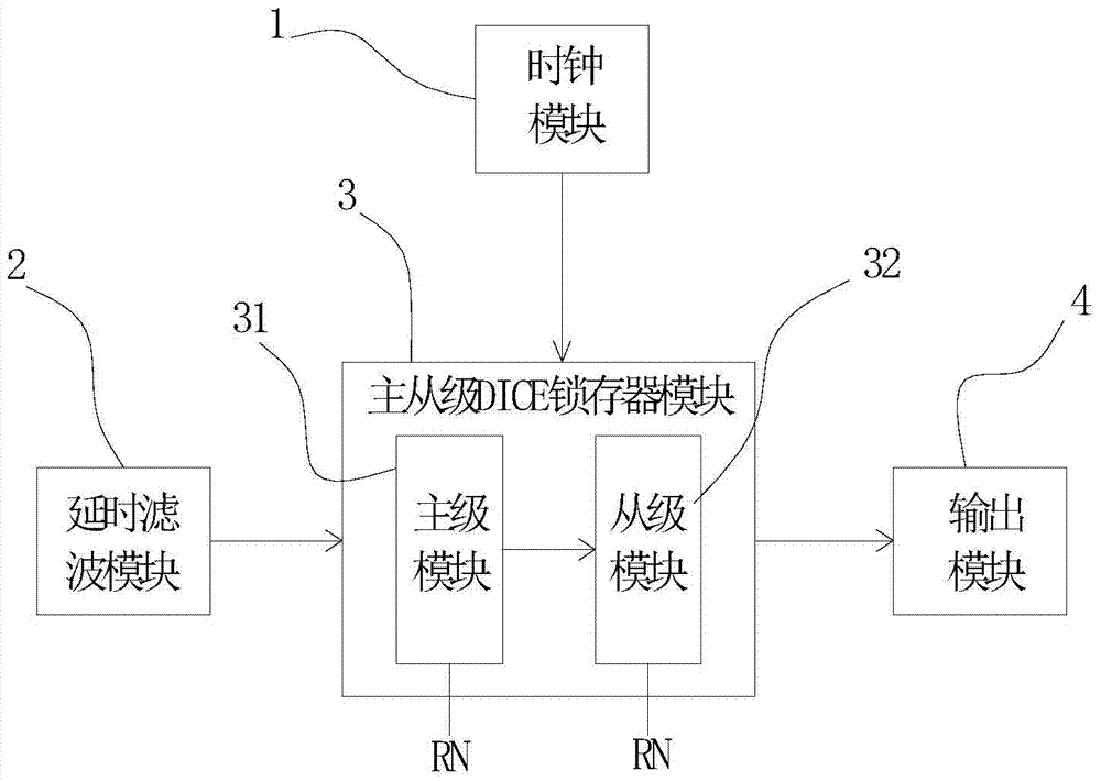
[0031] like figure 1 As shown, a D flip-flop with a reset terminal according to an embodiment of the present invention includes a clock module 1 , a delay filter module 2 , a master-slave DICE latch module 3 , and an output module 4 . The master-slave DICE latch module includes a master module 31 and a slave module 32 . Both the master and slave stages are reinforced with DICE, and a delay filter module 2 is added to the data end.
[0032] The clock signal output of the clock module 1 is connected to the clock signal input of the master-slave DICE latch module 3, the data input of the delay filter module 2 is connected to the data source, and the data output is connected to the master-slave DICE latch The data input end of the module 3 is connected, and the data output end of the master-slave DICE latch module 3 is connected to the signal input end of the output module 4 .
[...
PUM
 Abstract
Description
Claims
Application Information