Array substrate, display panel and display device

An array substrate and line segment technology, applied in the field of electronics, can solve the problems of permanent damage to electronic products, no clear release route, damage to electronic products, etc., and achieve the effects of preventing ESD damage, good electrostatic protection, and simple manufacturing process.

Active Publication Date: 2015-11-25
BOE TECH GRP CO LTD +1
View PDF4 Cites 13 Cited by
  • Summary
  • Abstract
  • Description
  • Claims
  • Application Information

AI Technical Summary

Problems solved by technology

[0003] There is no clear way to release the static electricity formed on electronic products. When the static electricity reaches a certain level, it will cause damage to electronic products.
In the prior art, the grounding point is made on the array substrate, and the static electricity on the substrate is discharged through a specific electrical connection; each discharge of static electricity will cause damage to components, but no irreversible damage is caused, so it can continue to work
But with the constant ESD bombardment, eventually the electronics will be permanently damaged

Method used


Image

  • Array substrate, display panel and display device
  • Array substrate, display panel and display device
  • Array substrate, display panel and display device

Examples


Embodiment Construction

[0023] In order to make the technical problems, technical solutions and advantages to be solved by the present invention clearer, the following will describe in detail with reference to the drawings and specific embodiments.

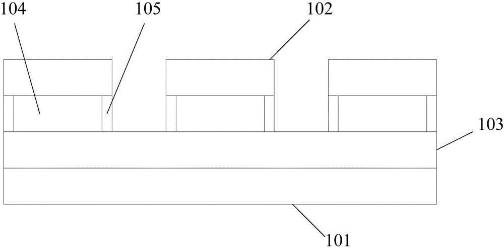
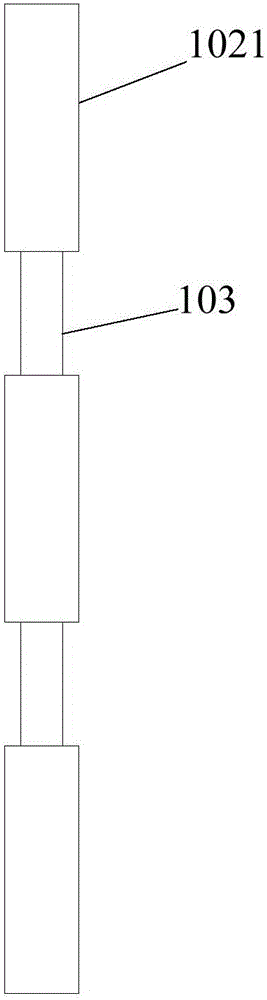
[0024] Such as figure 1 As shown, the present invention firstly provides an array substrate 101, including a first conductive pattern 102 and a second conductive pattern 103 constituting a GND protection circuit, the first conductive pattern 102 includes a plurality of first conductive line segments 1021 arranged at intervals, Adjacent first conductive line segments 1021 are connected by second conductive patterns 103, an insulating layer 104 is spaced between the first conductive line segments 1021 and the second conductive pattern 103, and the first conductive line segments 1021 and the The second conductive pattern 103 is connected through the via hole 105 penetrating through the insulating layer 104 .

[0025] A commonly used GND protection circuit ...


PUM


Abstract

The invention provides an array substrate, a display panel and a display device. The array substrate comprises a first conductive pattern and a second conductive pattern which form a GND (Ground) protection circuit, wherein the first conductive pattern comprises a plurality of first conductive line segments which are arranged at intervals; the adjacent first conductive line segments are connected through the second conductive pattern; insulating layers are spaced between the first conductive line segments and the second conductive pattern; and the first conductive line segments and the second conductive pattern are connected through penetrating through via holes of the insulating layers. Meanwhile, the invention provides the display panel, comprising the array substrate provided by any one embodiment of the invention. Furthermore, the invention further provides the display device comprising the array substrate provided by any one embodiment of the invention.

Description

technical field [0001] The present invention relates to the field of electronics, in particular to an array substrate, a display panel and a display device. Background technique [0002] There are two types of damage and damage caused by ESD (Electro-Static Discharge, electrostatic discharge) to electronic products: sudden damage and potential damage. Theoretically speaking, the GND (ground point) is located at the position of the IC (Integrated Circuit, integrated circuit), and at the GND, the probability of ESD damage to the Panel (display panel) is the smallest. However, according to the actual test results, the main location of the panel failure is concentrated near the GND. It can be considered that although the IC side is connected to the GND, the current generated by the ESD is too large and exceeds the protection capability of the GND. Therefore, it is inferred that the larger the edge equivalent resistance is, the easier it is for ESD to be derived through the GND ...

Claims


Application Information

Patent Timeline
Patent Type & Authority Applications(China)
IPC IPC(8): H01L27/12H01L23/60G09G3/20
CPCG09G3/20G09G2330/04G09G2330/06H01L27/0292H01L27/1244H01L23/60H01L27/12
Inventor 徐敬义杨波任艳伟刘宇赵欣赵艳艳赵二鹏王志强张伟
Owner BOE TECH GRP CO LTD
Why Eureka
Try Eureka