pixel structure

A technology of pixel structure and pixel unit, applied in the field of pixel structure, can solve the problems of short circuit of conductive structure and difficult realization of pixel design, and achieve the effect of avoiding short circuit and good component characteristics

Active Publication Date: 2019-01-01
AU OPTRONICS CORP
View PDF4 Cites 0 Cited by
  • Summary
  • Abstract
  • Description
  • Claims
  • Application Information

AI Technical Summary

Problems solved by technology

However, limited by the manufacturing process limit, the conductive structure in the pixel may be short-circuited due to the narrowing of the gap, making it difficult to realize high-resolution pixel design

Method used


Image

  • pixel structure
  • pixel structure
  • pixel structure

Examples


Embodiment Construction

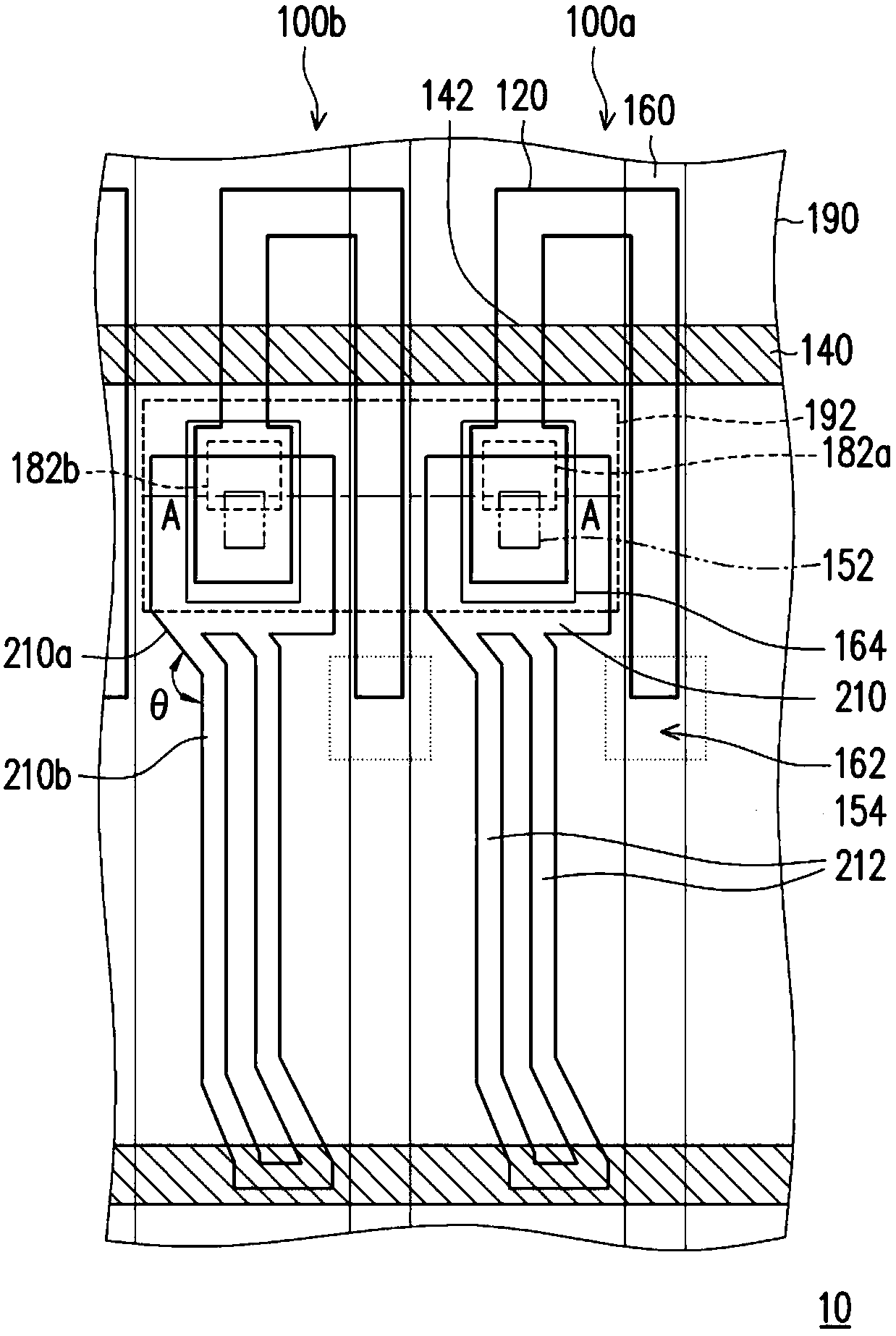
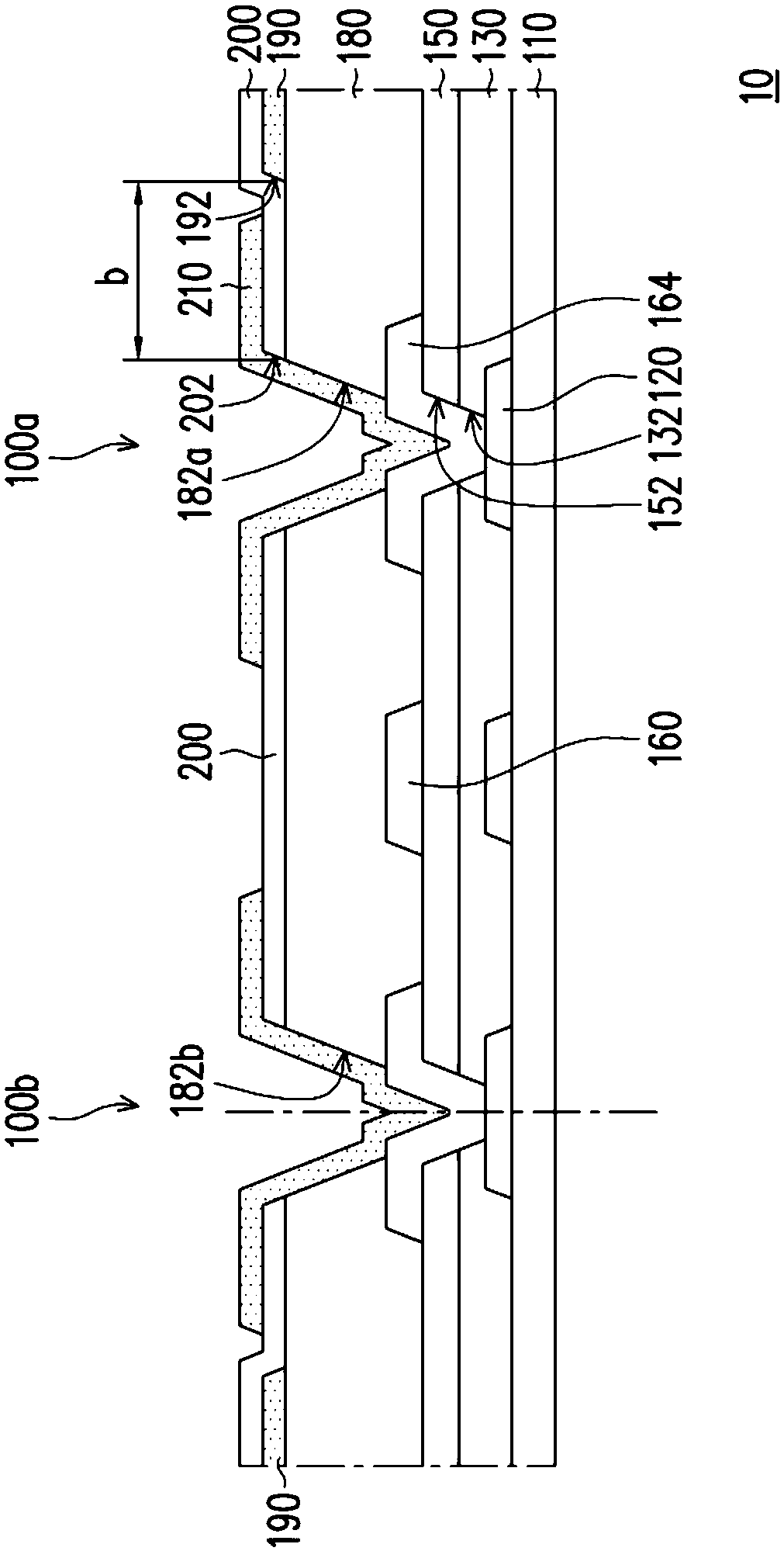
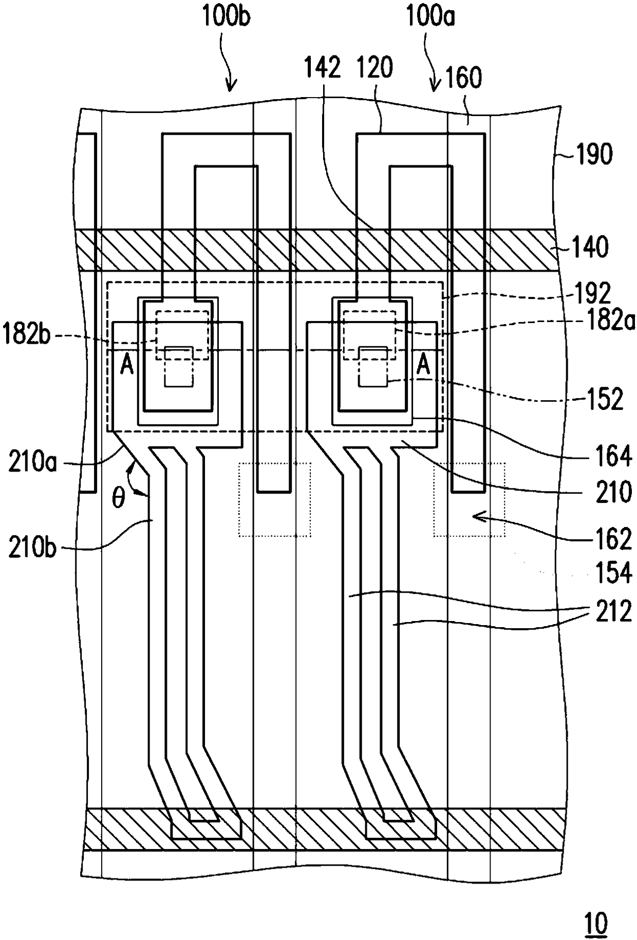
[0054] Figure 1A is a schematic diagram of a pixel structure according to an embodiment of the present invention, and Figure 1B is along Figure 1A The schematic cross-section of A-A'. Please also refer to Figure 1A and Figure 1B, in this embodiment, the pixel structure 10 includes a substrate 110 , two adjacent pixel units 100 a , 100 b , a first insulating layer 180 and a common electrode 190 . The third insulating layer 200 . The data line 160 is, for example, located between two adjacent pixel units 100a, 100b. In this embodiment, the data line 160 is taken as a straight line as an example, but the present invention does not take it as a line. In other embodiments, the data line 160 may also be a bent line or a line of other shapes.

[0055] In this embodiment, the pixel units 100a, 100b are located on the substrate 110, for example. The pixel units 100 a and 100 b include, for example, a gate 142 , a channel layer 120 , a source 162 and a drain 164 , and a pixel e...


PUM


Abstract

The invention discloses a pixel structure, which includes a first pixel unit, a second pixel unit, a first insulating layer and a common electrode. The first pixel unit is disposed on the substrate and includes a first drain and a first pixel electrode. The second pixel unit is disposed on the substrate and includes a second drain and a second pixel electrode. The first insulating layer covers the first drain and the second drain. The first pixel electrode and the second pixel electrode are disposed on the first insulating layer, and the first insulating layer has a first contact window opening exposing the first drain electrode and a second contact window opening exposing the second drain electrode. The common electrode is arranged on the first insulating layer and is electrically insulated from the first pixel electrode and the second pixel electrode. The common electrode has a common opening. On the vertical projection of the substrate, the opening of the first contact window and the opening of the second contact window both fall within the common opening.

Description

technical field [0001] The present invention relates to a pixel structure, and in particular to a pixel structure in which adjacent pixel units share a common opening of a common electrode. Background technique [0002] A head-mounted display (HMD) is a display worn on the body. A head-mounted display is a small display that is viewed through a lens set placed very close to the eyes, so it is actually similar to viewing a large display at a distance. Generally speaking, there are two ways of viewing a display, binocular and monocular, and the size of the display varies with the viewing method. In order to develop a head-mounted display that meets the requirements of thinness and lightness and is close to the eyes, it is necessary to further reduce the pixel size to increase the resolution of the display, so as to achieve the purpose of reducing the size of the display. However, limited by the limitation of the manufacturing process, the conductive structure in the pixel ma...

Claims


Application Information

Patent Timeline
Patent Type & Authority Patents(China)
IPC IPC(8): H01L27/12
CPCH01L27/1214H01L27/1244H01L27/1248G02F1/136227G02F1/134372H01L27/1225H01L27/124H01L27/156
Inventor 吕思慧苏志中李明贤
Owner AU OPTRONICS CORP
Why Eureka
Try Eureka