
Method for constructing floating gate

A floating gate and wafer technology, applied in the direction of semiconductor devices, etc., can solve problems such as FG short circuit and device failure

Active Publication Date: 2012-05-30
SEMICON MFG INT (SHANGHAI) CORP
View PDF2 Cites 0 Cited by
  • Summary
  • Abstract
  • Description
  • Claims
  • Application Information

AI Technical Summary

Problems solved by technology

Worse, too small spacing between FGs may cause a short circuit between adjacent FGs, resulting in device failure

Method used


Image

  • Method for constructing floating gate
  • Method for constructing floating gate
  • Method for constructing floating gate

Examples


Embodiment Construction

[0029] The inventors analyzed the existing FG construction process and found that the following factors may cause the distance between adjacent FGs to be too small:

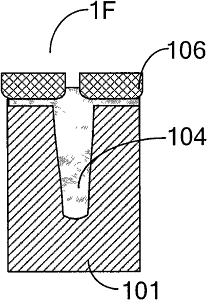
[0030] The process of removing silicon nitride is a wet etching process. In addition to removing silicon nitride 103, this process also has a corrosion effect on the silicon oxide filled in the STI, so that the volume of vacancies formed by the removed silicon nitride increases. . The subsequent two-step hydrofluoric acid pre-cleaning process further depleted the filled silicon oxide, and the width of the filled silicon oxide between the vacancies was reduced. From figure 1 This trend can be clearly seen from Section 1B to Section 1C in the figure. In this way, in the subsequent step of depositing polysilicon, the volume of polysilicon deposited in the vacancies is significantly larger than the volume of the original silicon nitride, and the width of the FG formed on this basis will also be too large, resultin...


PUM

PropertyMeasurementUnit
thicknessaaaaaaaaaa
thicknessaaaaaaaaaa

Abstract

The invention discloses a method for constructing a floating gate, comprising the following steps: A. successively depositing a silicon oxide film and a silicon nitride film on the upper surface of the silicon substrate of a wafer; B. defining a shallow trench graph on the wafer in the processes of shallow trench photoetching and silicon nitride etching; C. after the silicon oxide is deposited inthe shallow trench, carrying out first planarization processing on the upper surface of the wafer; D. removing the silicon nitride, forming a vacancy on the original position of the silicon nitride, forming a protective gap wall on the side wall of the silicon oxide, wherein the reaction rate of the protective gap wall and hydrofluoric acid is less than the reaction rate of the silicon oxide and the hydrofluoric acid; E. pre-cleaning the surface of the wafer by acid solution which takes the hydrofluoric acid as a main ingredient, growing a gate oxide layer on the surface of the wafer, and depositing polycrystalline silicon on the vacancy; and F. carrying out secondary planarization processing to the upper surface of the wafer, and mutually separating polycrystalline silicon in different vacancies to form the floating gate.

Description

technical field [0001] The invention relates to the technical field of semiconductor integrated circuit manufacturing, in particular to a method for constructing a floating gate. Background technique [0002] Self-aligned-Process (SAP) is widely used in flash memory because it can achieve good self-alignment performance between floating gate (Floating Gate, FG) and shallow trench isolation (Shallow Trench Isolation, STI). (flash memory) storage unit manufacturing process. [0003] figure 1 A schematic diagram showing changes in a typical structural section of a wafer during the manufacturing process of a data storage unit (bit-cell) of a split-gate (Split-Gate) memory in the prior art. The initial wafer is a silicon substrate, a silicon oxide film is deposited on the upper surface, and a silicon nitride film is deposited on the silicon oxide film. Through the STI etching (STI-ET)-process, a shallow trench pattern is defined on the wafer, and the fragment section with typi...

Claims


Application Information

Patent Timeline
Patent Type & Authority Patents(China)
IPC IPC(8): H01L21/28
Inventor 王友臻周儒领詹奕鹏
Owner SEMICON MFG INT (SHANGHAI) CORP
Learn More