Embedded touch panel and array substrate thereof

A technology for touch panels and array substrates, applied in optics, instruments, electrical digital data processing, etc., can solve the problems affecting the accuracy of touch signals and the decline of touch accuracy, and achieve increased work accuracy and resistance to capacitive loads. Effect of reduction, resistance value and capacitance value drop

Active Publication Date: 2017-02-22
WUHAN CHINA STAR OPTOELECTRONICS TECH CO LTD
View PDF5 Cites 13 Cited by
  • Summary
  • Abstract
  • Description
  • Claims
  • Application Information

AI Technical Summary

Problems solved by technology

In order not to affect the pixel aperture ratio, the metal connection line is generally arranged above the data line of the touch panel, so there will be a resistive capacitive load (RC Loading) between the metal connection line and the data line, and the load will affect The accuracy of the touch signal transmitted by the metal connection leads to a decrease in touch accuracy

Method used


Image

  • Embedded touch panel and array substrate thereof
  • Embedded touch panel and array substrate thereof
  • Embedded touch panel and array substrate thereof

Examples


Embodiment Construction

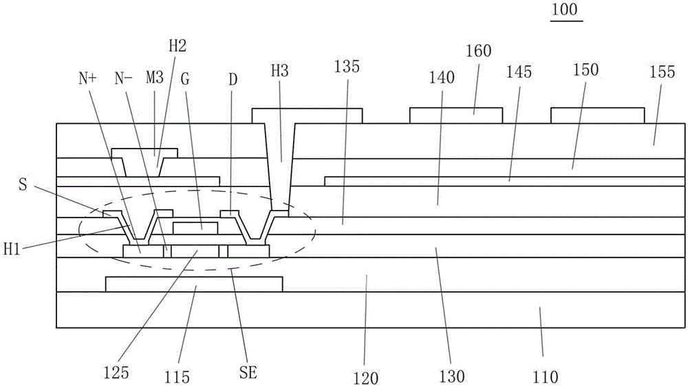
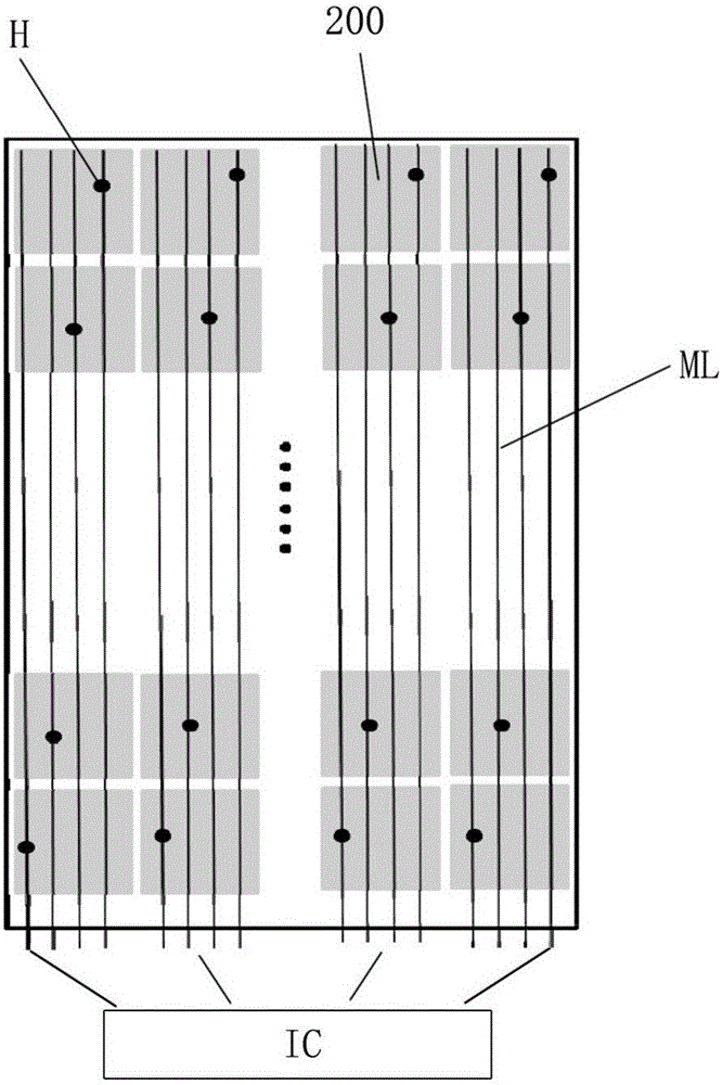
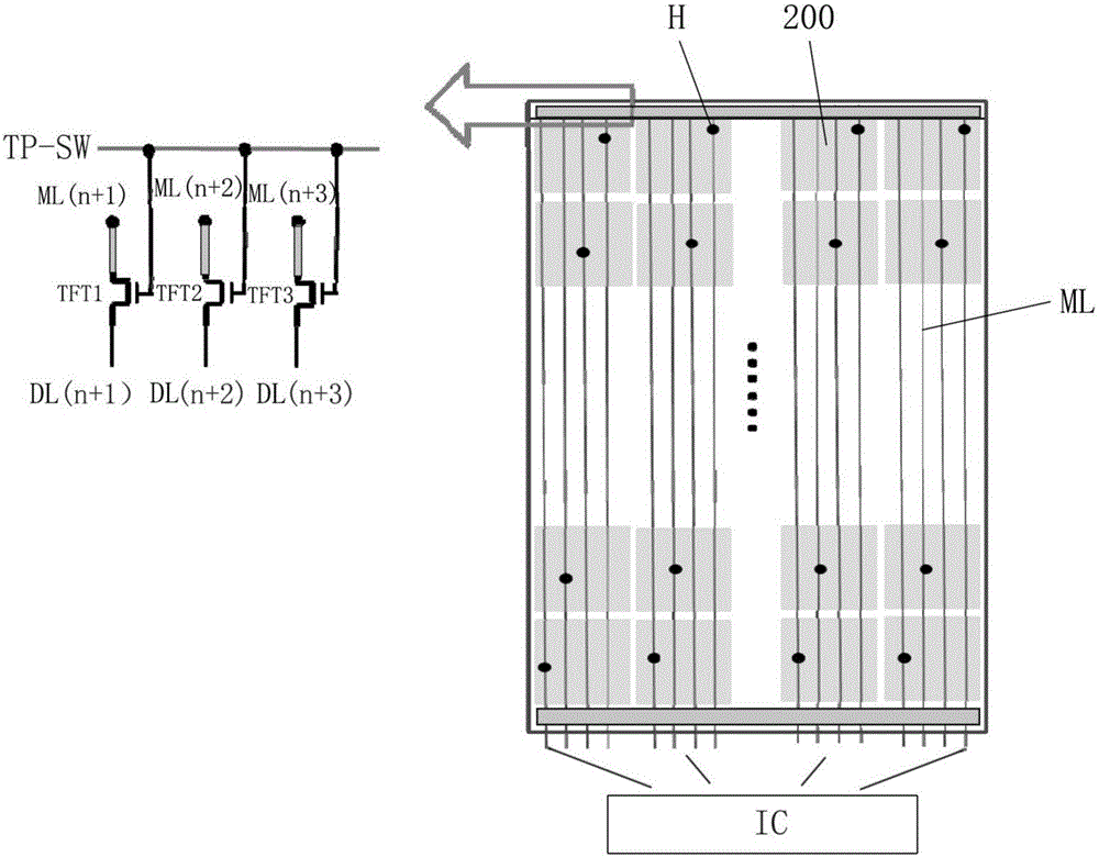
[0018] Hereinafter, the inventive concept will be described in detail by explaining exemplary embodiments with reference to the accompanying drawings. However, the inventive concepts may be embodied in many different forms and should not be construed as limited to the embodiments set forth herein; rather, these embodiments are provided so that this disclosure will be thorough and complete, and will inform the present Those of ordinary skill in the art fully convey the inventive concept. In the drawings, the same reference numerals denote the same elements. Furthermore, various elements and regions are shown schematically. Accordingly, the inventive concepts are not limited to the relative sizes or distances shown in the figures. It will be understood that although the terms first, second etc. may be used herein to describe various elements and / or components, these elements and / or components should not be limited by these terms. These terms are only used to distinguish one e...


PUM


Abstract

The invention provides an array substrate of an embedded touch panel. The array substrate comprises touch electrodes, touch sensing chips and metal connecting lines, wherein the touch electrodes are arranged in an active region of the touch panel in an array manner; the touch sensing chips are arranged outside the active region of the touch panel; the metal connecting lines and the touch electrodes are arranged on different layers, and the metal connecting lines are connected to the touch electrodes through via holes; the metal connecting lines and data lines of the touch panel are stacked mutually in an insulating manner; the touch electrodes are connected to the touch sensing chips through the metal connecting lines; a switching circuit is arranged between the metal connecting lines and the data lines; and the switching circuit is used for conducting the metal connecting lines and the data lines at a touch phase, and disconnecting the metal connecting lines and the data lines at a display phase. The resistance and capacitance load of cabling in the active region of the touch panel is reduced, so that the working precision of the touch panel is improved.

Description

technical field [0001] The present invention relates to a touch panel, in particular to an in-cell touch panel and an array substrate thereof. Background technique [0002] Liquid crystal display (Liquid Crystal Display, LCD) is the most widely used flat panel display at present, and has gradually become a variety of devices such as mobile phones, personal digital assistants (PDAs), digital cameras, desktop computers or laptop computers A display with a high-resolution color screen used in electronic equipment. [0003] With the development and progress of liquid crystal display technology, people put forward higher requirements for LCD display quality, appearance design, human-machine interface, etc. hotspots. [0004] Touch technology has developed rapidly in recent years, and various touch panels have been put into mass production. For the existing touch panel, according to the position of the touch sensor (Touch Sensor), it can be divided into the type where the touch...

Claims


Application Information

Patent Timeline
Patent Type & Authority Applications(China)
IPC IPC(8): G06F3/041G02F1/1333
CPCG02F1/13338G06F3/041G06F3/0412G06F3/0443G02F1/134363G02F1/136209G02F1/136227G02F1/136286G02F1/1368G02F1/13606G02F1/13685
Inventor 张启沛张春倩
Owner WUHAN CHINA STAR OPTOELECTRONICS TECH CO LTD
Why Eureka
Try Eureka