Multi-lens camera module sharing photosensitive chip and electronic device

A technology of camera module and photosensitive chip, which is applied in the direction of TV, electrical components, color TV, etc., and can solve the problem of small shooting angle of camera module

CN107343128AInactive Publication Date: 2017-11-10TRULY OPTO ELECTRONICS
3 Cites 8 Cited by

Patent Information

Authority / Receiving Office
CN · China
Current Assignee / Owner
Publication Date
2017-11-10
Estimated Expiration
Not applicable · inactive patent

Smart Images

  • Figure 1
    Figure 1
  • Figure 2
    Figure 2
  • Figure 3
    Figure 3
Patent Text Reader

Abstract

The invention discloses a multi-lens camera module sharing a photosensitive chip and an electronic device. The multi-lens camera module includes a framing element which has a top surface and a bottom surface that are oppositely and parallelly arranged; at least one side surface connecting to the bottom surface and the top surface; a photosensitive chip disposed opposite to the bottom surface; a main lens opposite to the top surface; and at least one auxiliary lens; wherein the light information collected by the main lens sequentially passes through the top surface and the bottom surface and is incident to the set area of the photosensitive chip, the auxiliary lens is in one-to-one correspondence with the side surface, the light information collected by the auxiliary lens is reflected by the corresponding side surface, and is incident to the set area of the photosensitive chip, and the light information collected by different lenses is incident to the different areas of the photosensitive chip. According to the invention, different lenses have different market angles, and the shooting angles are greatly increased.
Need to check novelty before this filing date? Find Prior Art

Description

technical field

[0001] The invention relates to the technical field of imaging devices, more specifically, to a multi-lens camera module and electronic equipment that share a photosensitive chip. Background technique

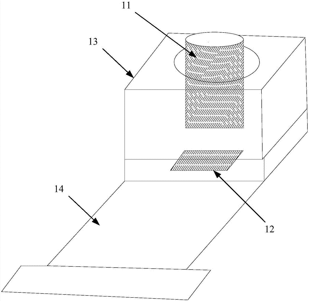
[0002] With the continuous development of science and technology, more and more electronic devices with image acquisition functions are widely used in people's daily life and work, which brings great convenience to people's daily life and work, and has become an indispensable essential tool. The main component of the camera image acquisition function of electronic equipment is the camera module, and the existing camera modules are generally as follows figure 1 shown.

[0003] refer to figure 1 , figure 1 It is a schematic structural diagram of a common camera module in the prior art. The existing camera module includes: a photosensitive chip 12 and a lens 11 arranged opposite to each other. The lens 11 is located in the motor 13 , and the photosensitive c...

Examples

Embodiment Construction

[0029] The following will clearly and completely describe the technical solutions in the embodiments of the present invention with reference to the accompanying drawings in the embodiments of the present invention. Obviously, the described embodiments are only some, not all, embodiments of the present invention. Based on the embodiments of the present invention, all other embodiments obtained by persons of ordinary skill in the art without making creative efforts belong to the protection scope of the present invention.

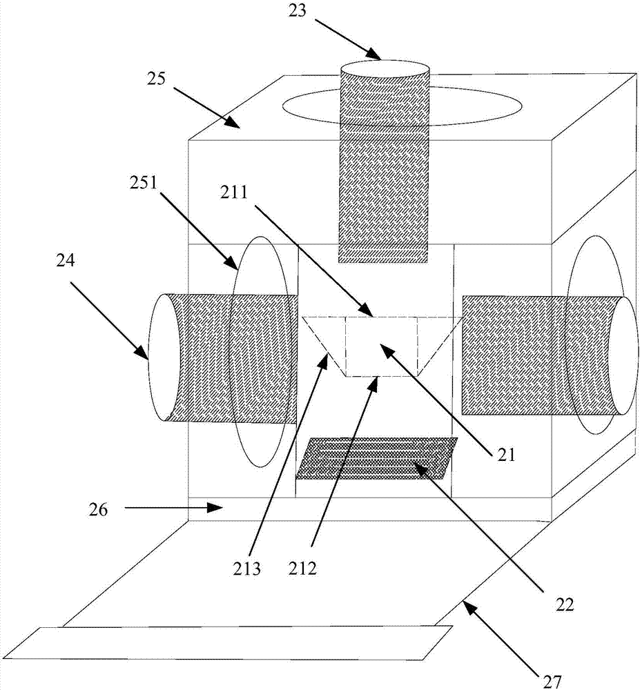
[0030] In order to make the above objects, features and advantages of the present invention more comprehensible, the present invention will be further described in detail below in conjunction with the accompanying drawings and specific embodiments.

[0031] refer to figure 2 , figure 2 It is a schematic structural diagram of a multi-lens camera module sharing a photosensitive chip provided by an embodiment of the present invention, figure 2 The shown mult...