Method for making thin film transistor

A technology of thin-film transistors and manufacturing methods, which is applied in the field of liquid crystal display, can solve problems such as increasing the difficulty of mass production, changes in mass production conditions, and harshness, and achieve the effects of improving leakage problems and optimizing process flow

Active Publication Date: 2017-12-15
WUHAN CHINA STAR OPTOELECTRONICS TECH CO LTD
View PDF5 Cites 16 Cited by
  • Summary
  • Abstract
  • Description
  • Claims
  • Application Information

AI Technical Summary

Problems solved by technology

The above-mentioned technological means lead to more stringent changes in mass production conditions, which will affect the development and mass production cycle of the display panel copper process and increase the difficulty of mass production

Method used


Image

  • Method for making thin film transistor
  • Method for making thin film transistor
  • Method for making thin film transistor

Examples


Embodiment Construction

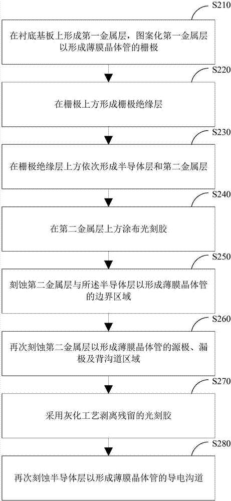
[0025] The implementation of the present invention will be described in detail below in conjunction with the accompanying drawings and examples, so as to fully understand and implement the implementation process of how to apply technical means to solve technical problems and achieve corresponding technical effects in the present invention. The embodiments of the present application and the various features in the embodiments can be combined with each other under the premise of no conflict, and the formed technical solutions are all within the protection scope of the present invention.

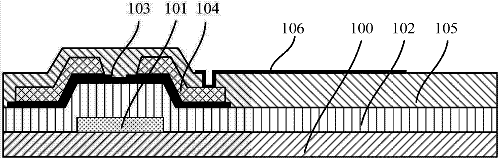
[0026] figure 1 It is a schematic diagram of the film layer structure of the thin film transistor on the display panel. As shown in the figure, 100 is the glass substrate of the display panel. An insulating layer 102, a semiconductor layer 103, and the source and drain electrodes 104 of the thin film transistor (ie, the second metal layer). An insulating protection layer 105 is covered on the ...


PUM


Abstract

The present invention discloses a method for making a thin film transistor. The method is applied to a display panel copper process. The method comprises a step of forming a first metal layer on a substrate and patterning the first metal layer to form a gate electrode of the thin film transistor, a step of forming a gate insulating layer on the gate, a step of orderly forming a semiconductor layer and a second metal layer on the gate insulating layer, a step of coating the second metal layer with a photoresist, a step of etching the second metal layer and the semiconductor layer to form a border region of the thin film transistor, a step of etching the second metal layer again to form a source electrode, a drain electrode and a back channel region of the thin film transistor, a step of using ashing process to peeling remaining photoresist, and a step of etching the semiconductor layer again to form a conductive channel of the thin film transistor. According to the method, an electric leakage problem of the thin film transistor caused by factors of the diffusion of copper, the pollution of an organic stripping solution and the like is improved.

Description

technical field [0001] The invention belongs to the technical field of liquid crystal display, and in particular relates to a manufacturing method of a thin film transistor. Background technique [0002] With the development of Flat Panel Display (FPD) technology, people's pursuit of display resolution and frame refresh rate is getting higher and higher, so the development of new materials and new processes is imminent. [0003] At present, in the field of liquid crystal display (TFT LCD) processing and manufacturing, the materials of the conductive layer metal are mainly aluminum and molybdenum. The advantages of aluminum and molybdenum are that the film forming process is simple, the adhesion and flatness are good, and they are soft and non-toxic. It is prone to climbing disconnection and difficult to diffuse (diffusion leads to membrane pollution). Aluminum is the ideal conductive metal material of choice for small size and low resolution panels. However, due to the rel...

Claims


Application Information

Patent Timeline
Patent Type & Authority Applications(China)
IPC IPC(8): H01L21/336
CPCH01L29/66765H01L27/1288H01L29/78669H01L29/4908H01L21/32139H01L21/31138H01L27/127G02F1/136227G02F1/133345H01L29/41733H01L27/1214H01L29/458H01L29/78609H01L29/42384H01L29/78603H05K2201/0338H01L29/518H01L2924/13069H01L21/0274H01L21/32G03F7/0035G03F1/80H01L29/78618G03F7/0041G03F5/16H01L21/31144H05K2201/0361H01L21/31058H01L21/30604H01L21/32134H01L21/3085H01L21/31133H01L21/3086H01L21/3065H01L21/3081H01L21/2855H01L21/0217H01L21/02274H01L21/0262H01L21/02592B81C2201/0108G03F7/422G03F7/427
Inventor 孙涛
Owner WUHAN CHINA STAR OPTOELECTRONICS TECH CO LTD
Why Eureka
Try Eureka