

Thin film transistor device and preparation method thereof
A thin-film transistor and device technology, applied in the field of thin-film transistor devices and their preparation, can solve problems such as unregulated, poor display effect of display devices, and poor electrical characteristics of thin-film transistor devices, so as to increase the turn-on current and improve the display effect , Enhance the effect of electrical characteristics
- Summary
- Abstract
- Description
- Claims
- Application Information
AI Technical Summary
Problems solved by technology
Method used
Image

Examples
Embodiment Construction
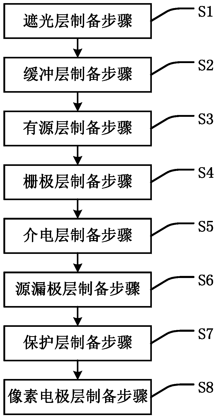
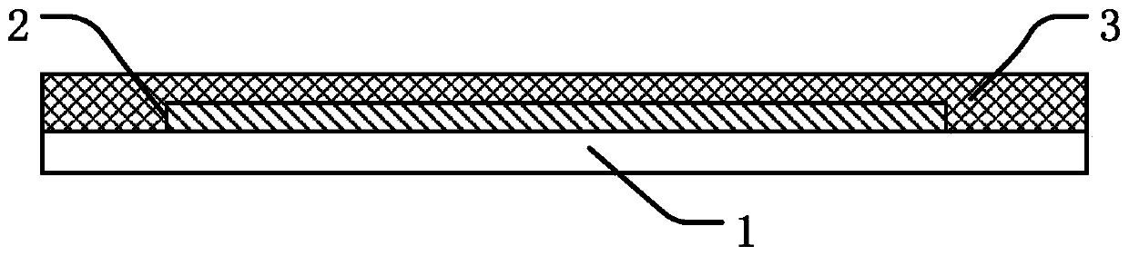
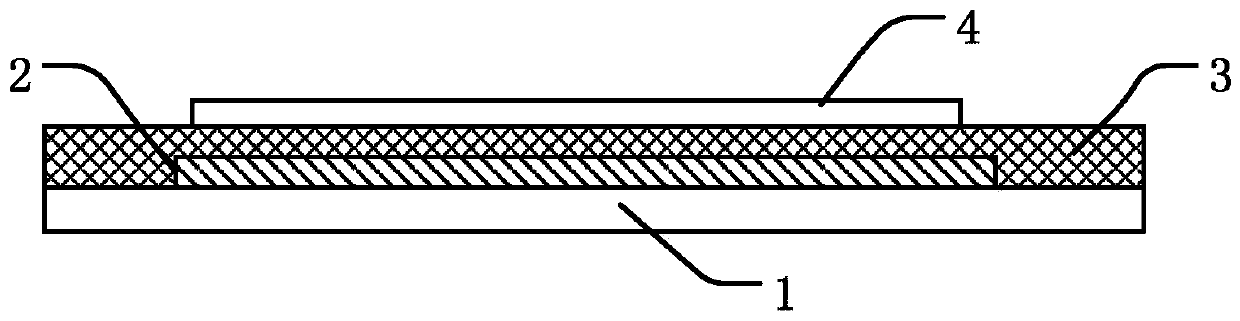
[0029] The preferred embodiments of the present invention will be described in detail below in conjunction with the accompanying drawings, to fully introduce the technical content of the present invention to those skilled in the art, to prove that the present invention can be implemented, to make the technical content disclosed in the present invention clearer, and to make the technical content of the present invention clearer. It is easier for those skilled in the art to understand how to implement the present invention. However, the present invention can be realized through many different forms of embodiments, and the scope of protection of the present invention is not limited to the embodiments mentioned herein, and the descriptions of the following embodiments are not intended to limit the scope of the present invention.
[0030] The directional terms mentioned in the present invention, such as "up", "down", "front", "back", "left", "right", "inside", "outside", "side", etc...
PUM
 Abstract
Description
Claims
Application Information