Pixel arrangement structure, manufacturing method, display panel and display device

A technology of pixel arrangement and manufacturing method, which is applied in semiconductor/solid-state device manufacturing, electrical components, electrical solid-state devices, etc., can solve the problem that the luminous efficiency of G material cannot be maximized, and the display brightness and display effect are affected. Luminous brightness and effects, effects that increase brightness

Inactive Publication Date: 2019-11-01
SUZHOU QUINGYUE OPTOELECTRONICS TECH CO LTD
View PDF6 Cites 6 Cited by
  • Summary
  • Abstract
  • Description
  • Claims
  • Application Information

AI Technical Summary

Problems solved by technology

[0004] In view of this, embodiments of the present invention provide a pixel arrangement structure and manufacturing method, a display panel, and a display device to solve the problem th

Method used


Image

  • Pixel arrangement structure, manufacturing method, display panel and display device
  • Pixel arrangement structure, manufacturing method, display panel and display device
  • Pixel arrangement structure, manufacturing method, display panel and display device

Examples


Example Embodiment

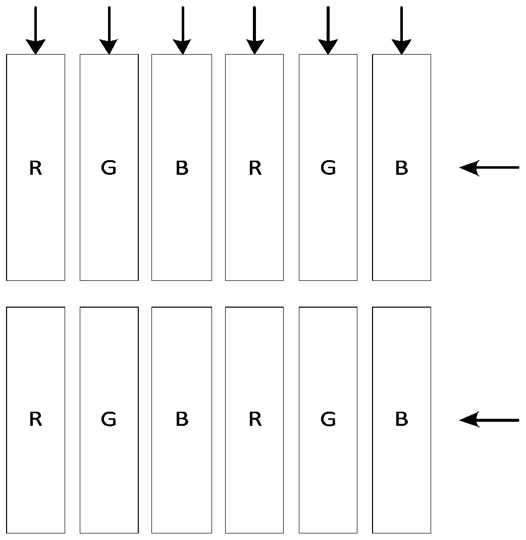
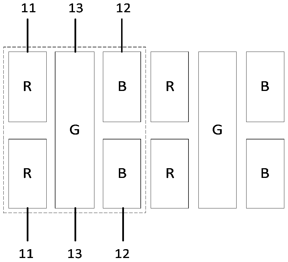
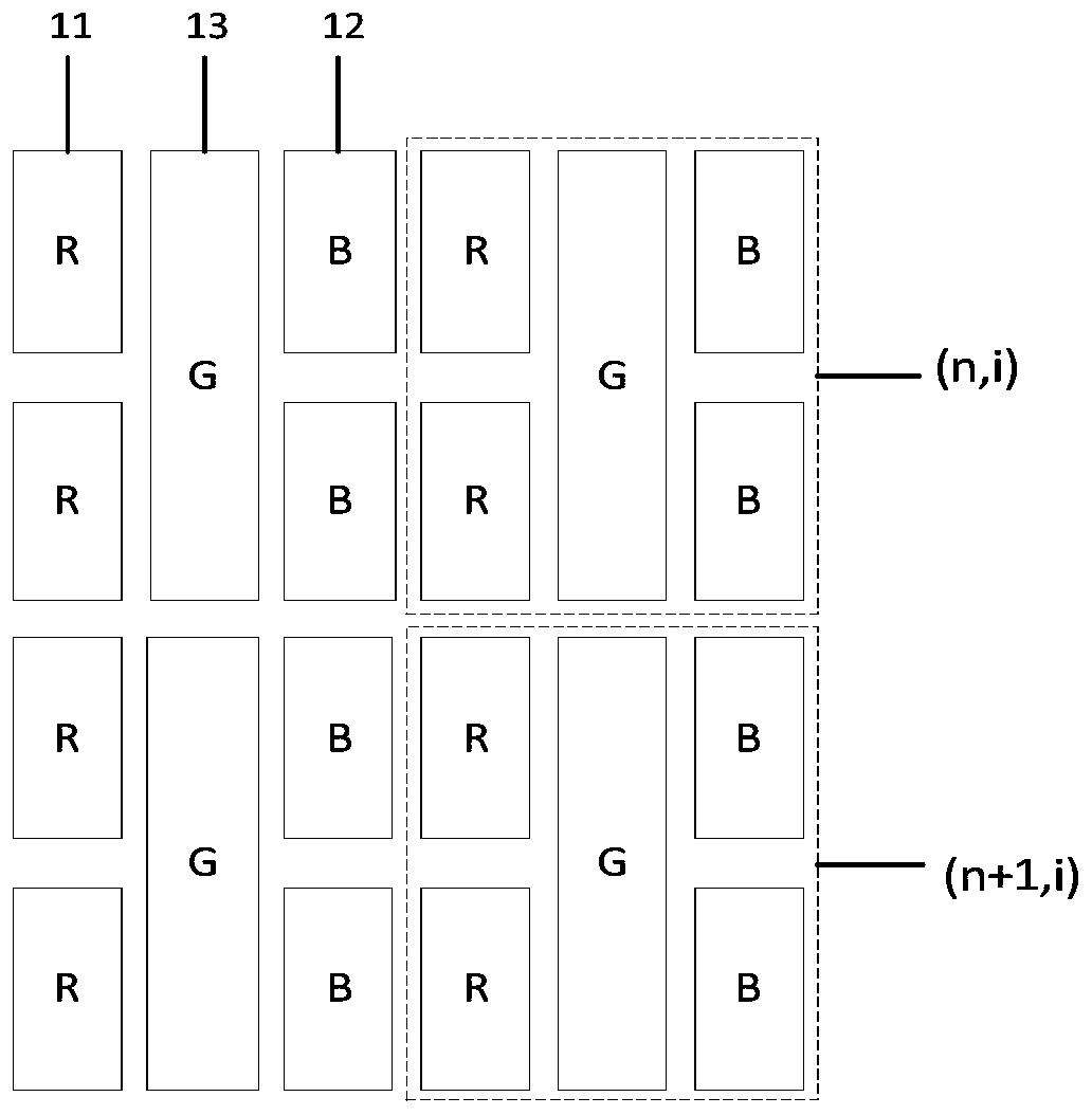
[0025] In order to make the object, technical solution and advantages of the invention clearer, the present invention will be further described in detail below in conjunction with the accompanying drawings and embodiments. It should be understood that the specific embodiments described here are only used to explain the present invention, not to limit the present invention.

[0026] In describing the present invention, it should be understood that the terms "central", "lateral", "upper", "lower", "left", "right", "vertical", "horizontal", "top", " The orientation or positional relationship indicated by "bottom", "inner" and "outer" is based on the orientation or positional relationship shown in the drawings, and is only for the convenience of describing the present invention and simplifying the description, rather than indicating or implying the referred device or Elements must have certain orientations, be constructed and operate in certain orientations, and therefore should n...


PUM


Abstract

The invention discloses a pixel arrangement structure, a manufacturing method, a display panel and a display device. The pixel arrangement structure comprises a plurality of pixel units. The sub-pixelof each pixel unit comprises two first sub-pixels, two second sub-pixels and a third sub-pixel. The light-emitting area of the third sub-pixel is larger than the sum of the light-emitting areas of the two first sub-pixels, and the light-emitting area of the third sub-pixel is larger than the sum of the light-emitting areas of the two second sub-pixels. The luminous efficiency of the green material is higher than those of the red material and the blue material. The brightness is inversely proportional to the light-emitting area. Therefore, according to the pixel arrangement structure providedby the embodiment of the invention, the light emitting areas of the red sub-pixels and the blue sub-pixels are reduced. The brightness of the red sub-pixel and the blue sub-pixel is improved, so thatthe pixel unit composed of the red sub-pixel, the blue sub-pixel and the green sub-pixel makes full use of the luminous efficiency of the three sub-pixels when emitting white light. The luminous brightness and the effect of the pixel units are improved.

Description

technical field [0001] The invention relates to the field of display technology, in particular to a pixel arrangement structure and a manufacturing method, a display panel, and a display device. Background technique [0002] OLED display technology has the characteristics of self-luminescence, wide viewing angle, high contrast, low power consumption, high response rate, light weight, thin thickness, full color, simple manufacturing process, etc., and is a representative of cutting-edge technology. According to the driving method, OLED can be divided into two types: active drive (AMOLED) and passive drive (PMOLED). Among them, PMOLED has a simple structure and easy manufacturing process, can effectively reduce manufacturing costs, and has a very fast response speed, and has great development potential in displaying simple micro-devices. When PMOLED is displayed, its display module is composed of three colors of red (R), green (G), and blue (B), and the display effect is rela...

Claims


Application Information

Patent Timeline
IPC IPC(8): H01L27/32H01L51/56
CPCH10K59/352H10K59/353H10K59/17H10K71/00
Inventor 陶林刘宏俊
Owner SUZHOU QUINGYUE OPTOELECTRONICS TECH CO LTD
Why Eureka
Try Eureka