A level processing circuit, a gate drive circuit, and a display device

A technology for processing circuits and circuits, which is applied in the field of level processing circuits, display devices, and gate drive circuits. Horizontal stripes, the effect of solving static electricity residue

Active Publication Date: 2022-03-25
FUZHOU BOE OPTOELECTRONICS TECH CO LTD +1
View PDF12 Cites 0 Cited by
  • Summary
  • Abstract
  • Description
  • Claims
  • Application Information

AI Technical Summary

Problems solved by technology

[0003] In a low-temperature environment, due to changes in parameters such as the reverse turn-off time and reverse turn-off voltage of the parasitic diode of the thin film transistor, the liquid crystal equivalent capacitance C of the display device LC and storage capacitor C S The residual charge cannot be released through the thin film transistor in a short time, and will slowly accumulate over time, thus showing the limit power sequence (Limit Power Sequence, referred to as LPS) stripes ( figure 1 )The phenomenon
That is, the performance of the thin film transistor included in the sub-pixel deteriorates in a low-temperature environment, and the electron mobility deteriorates correspondingly, so that different degrees of residual charges occur in different positions of the display screen, which in turn causes LPS stripes to appear on the display screen of the display device.

Method used


Image

  • A level processing circuit, a gate drive circuit, and a display device
  • A level processing circuit, a gate drive circuit, and a display device
  • A level processing circuit, a gate drive circuit, and a display device

Examples


Embodiment Construction

[0026] The technical solutions in the embodiments of the present invention will be clearly and completely described below with reference to the accompanying drawings in the embodiments of the present invention. Obviously, the described embodiments are only a part of the embodiments of the present invention, but not all of the embodiments. Based on the embodiments of the present invention, all other embodiments obtained by those of ordinary skill in the art without creative efforts shall fall within the protection scope of the present invention.

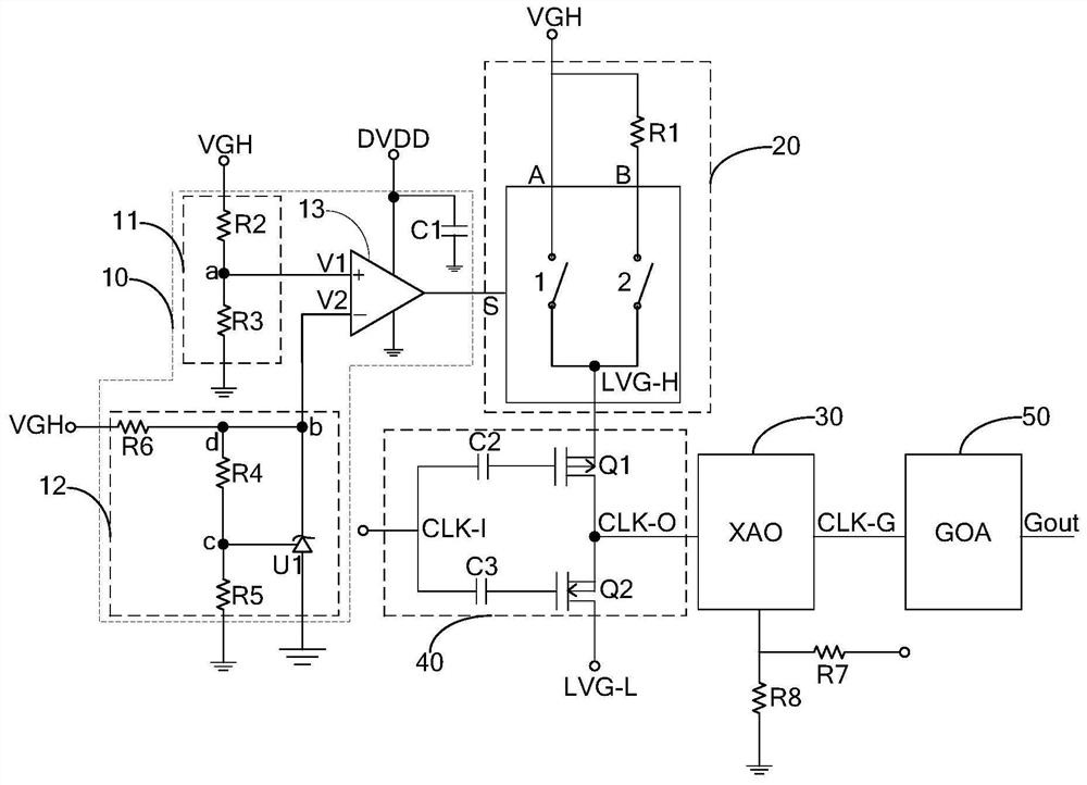
[0027] The display device includes an array substrate, the array substrate includes a display area and a peripheral area located at the periphery of the display area, and the display area includes a plurality of sub-pixels, gate lines, data lines and the like. The sub-pixel includes a pixel circuit, and the pixel circuit may include a thin film transistor as a switching element, a pixel electrode, a common electrode, and the like. The...


PUM


Abstract

Embodiments of the present invention provide a level processing circuit, a gate drive circuit, and a display device, which relate to the field of display technology and can solve the problem of LPS stripes on the display device when the device is shut down in a low temperature environment. A level processing circuit includes a voltage detection circuit, a switch selection circuit, and an XAO circuit; the voltage detection circuit is configured to output a high level to the switch selection circuit if the first voltage is greater than or equal to the second voltage; if the first If the voltage is less than the second voltage, the low level is output to the switch selection circuit; the switch selection circuit includes a first switch and a second switch connected in parallel, and the second switch includes a first sub-switch and a first resistor connected in series; the configuration of the switch selection circuit It is: if the voltage detection circuit outputs a high level, the first switch is turned on, and the high level is output to the XAO circuit; if the voltage detection circuit outputs a low level, the first sub-switch is turned on, and the low level is output to the XAO circuit. XAO circuit.

Description

technical field [0001] The present invention relates to the field of display technology, and in particular, to a level processing circuit, a gate driving circuit and a display device. Background technique [0002] Currently, when testing products with high refresh rate and high resolution, for example, at a temperature of -5° C., the display device is turned on and off every 3 seconds. [0003] In the low temperature environment, due to the change of the parameters such as the reverse turn-off time and reverse turn-off voltage of the parasitic diode of the thin film transistor, the liquid crystal equivalent capacitance C of the display device is changed. LC and storage capacitor C S The residual charge cannot be released cleanly through the thin film transistor in a short period of time, and will accumulate slowly over time, thus showing the Limit Power Sequence (LPS) horizontal stripes ( figure 1 )The phenomenon. That is, the performance of the thin film transistors incl...

Claims


Application Information

Patent Timeline
Patent Type & Authority Patents(China)
IPC IPC(8): G09G3/36
CPCG09G3/3696G09G3/3677
Inventor 陈信刁凯侯清娜陈美珍胡晔查文余仁惠郑上涛谢洪洲
Owner FUZHOU BOE OPTOELECTRONICS TECH CO LTD
Why Eureka
Try Eureka