Display panel pixel repairing light path system and display panel pixel repairing method

A display panel, pixel repair technology, applied in static indicators, instruments, etc., can solve the problem of unclear sub-pixel processing accuracy, and achieve the effect of reducing laser spot, clear structure, and improving processing accuracy

Pending Publication Date: 2021-03-19
苏州科韵激光科技有限公司
View PDF6 Cites 0 Cited by
  • Summary
  • Abstract
  • Description
  • Claims
  • Application Information

AI Technical Summary

Problems solved by technology

[0004] However, the existing repair systems are mainly aimed at repairing display panels with large single sub-pixels, such as display panels for mobile phones and computers, where the size of a single sub-pixel is on the order of more than ten microns
If the existing repair system is used to repair smaller-sized sub-pixels, there will be problems such as unclear sub-pixels and low processing accuracy.

Method used


Image

  • Display panel pixel repairing light path system and display panel pixel repairing method
  • Display panel pixel repairing light path system and display panel pixel repairing method
  • Display panel pixel repairing light path system and display panel pixel repairing method

Examples


Embodiment Construction

[0036] The present invention will be further described in detail below in conjunction with the accompanying drawings and embodiments. It should be understood that the specific embodiments described here are only used to explain the present invention, but not to limit the present invention. In addition, it should be noted that, for the convenience of description, only some structures related to the present invention are shown in the drawings but not all structures.

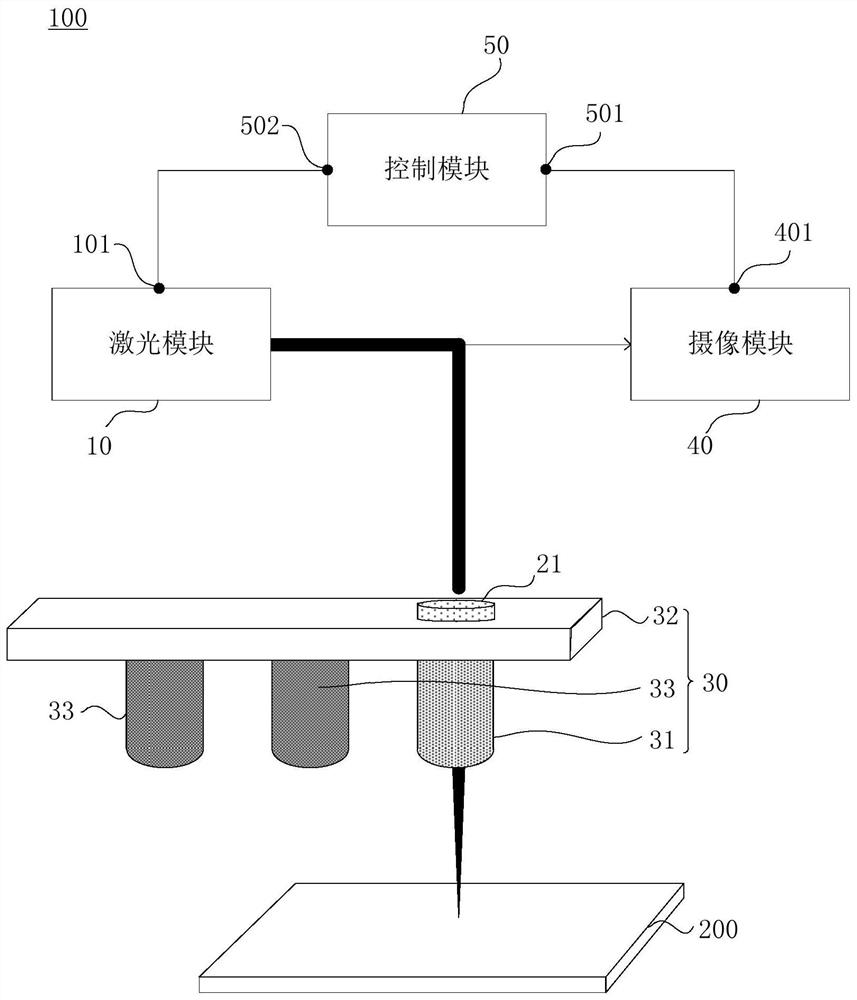
[0037] figure 1 It is a schematic structural diagram of a display panel pixel repair optical path system provided by an embodiment of the present invention, see figure 1 , the display panel pixel repair optical path system 100 provided by the embodiment of the present invention includes: a laser module 10, a first diaphragm 21, an objective lens module 30, a camera module 40 and a control module 50; Electrically connected; the objective lens module 30 includes a first objective lens 31, and the magnification of t...


PUM

PropertyMeasurementUnit
sizeaaaaaaaaaa
sizeaaaaaaaaaa

Abstract

The embodiment of the invention discloses a display panel pixel repair light path system and a display panel pixel repair method. The display panel pixel repair light path system comprises a laser module, a first diaphragm, an objective lens module, a camera module and a control module, wherein the camera module and the laser module are electrically connected with the control module; the objectivelens module comprises a first objective lens, and the magnification factor of the first objective lens is greater than or equal to 100*; the camera module is used for observing the display panel through the first diaphragm and the first objective lens so as to determine the position information of a defective sub-pixel and sending the position information to the control module; and the control module is used for controlling the laser module to emit a laser beam and controlling the direction of the laser beam emitted by the laser module according to the position information, so that the laserbeam sequentially passes through the first diaphragm and the first objective lens and then focuses on the defective sub-pixel to repair the defective sub-pixel. The display panel pixel repair light path system has high processing precision.

Description

technical field [0001] Embodiments of the present invention relate to a display panel repair technology, and in particular, to a display panel pixel repair optical path system and a display panel pixel repair method. Background technique [0002] With the continuous development of science and technology, the display industry has continued to improve its technical level from the first picture tube display, to the later LCD screen display, to LED, OLED, and now to AMOLED, QLED, Mini LED, Micro LED, etc. [0003] In the prior art, repairing technology is usually used to repair display panels with a small number of defects, so as to improve the yield and avoid waste. For example, repair technologies mainly include cathode isolation (Isolation), direct carbonization (Burning) and single point processing (Single Shot) and other technologies. [0004] However, the existing repair systems are mainly for repairing display panels with large single sub-pixels, such as display panels f...

Claims


Application Information

Patent Timeline
Patent Type & Authority Applications(China)
IPC IPC(8): G09G3/20
CPCG09G3/2074
Inventor 董岱杨军郝帅郎经纬
Owner 苏州科韵激光科技有限公司
Why Eureka
Try Eureka