
Flash memory device capable of improving reliability
a flash memory and reliability technology, applied in static storage, digital storage, instruments, etc., can solve problems such as read failure, program/erase (pe) endurance, and stress on the oxide layer of a cell transistor, and achieve the effect of reducing the disturbance of reads
- Summary
- Abstract
- Description
- Claims
- Application Information
AI Technical Summary
Benefits of technology
Problems solved by technology
Method used
Image



Examples
Embodiment Construction
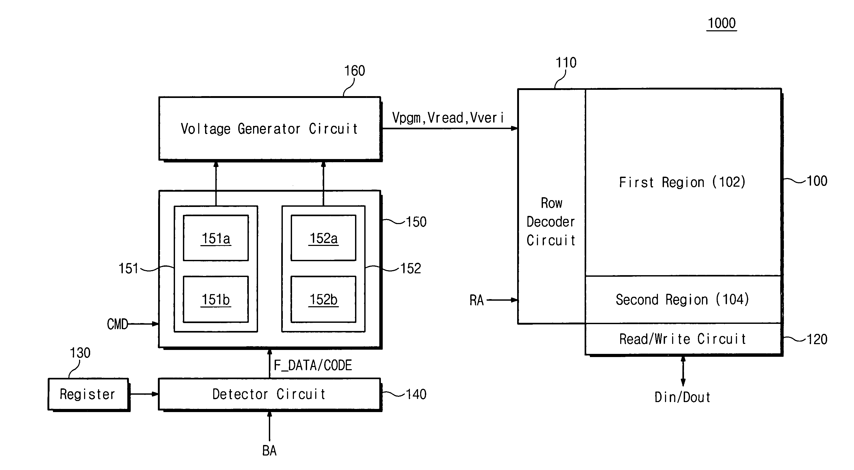
[0031]FIG. 4 is a block diagram of a flash memory device according to an embodiment of the present invention. As shown in FIG. 4, the flash memory device 1000 of the present invention includes a memory cell array 100 storing data information. The memory cell array 100 consists of first and second regions 102 and 104. The first region 102 is a data storage region for storing data, and the second region 104 is a code storage region for storing code. Each of the first and second regions 102 and 104 is formed of one or more memory blocks.
[0032] A memory block BLK of the memory cell array 100 is shown in FIG. 5 and includes a plurality of cell strings 10, referred to as a “NAND string”, respectively corresponding to bit lines BL0˜BLn-1. Each of the cell strings 10 consists of a string selection transistor SST as a first selection transistor, a ground selection transistor GST as a second selection transistor, and a plurality of memory cells MCm-1˜MC0. The plurality of the memory cells MC...
PUM
 Login to View More
Abstract
Description
Claims
Application Information
 Login to View More