

Semiconductor imaging device
- Summary
- Abstract
- Description
- Claims
- Application Information
AI Technical Summary
Benefits of technology
Problems solved by technology
Method used
Image

Examples
first embodiment
[0054] (Overall Arrangement of the CMOS Image Sensor)
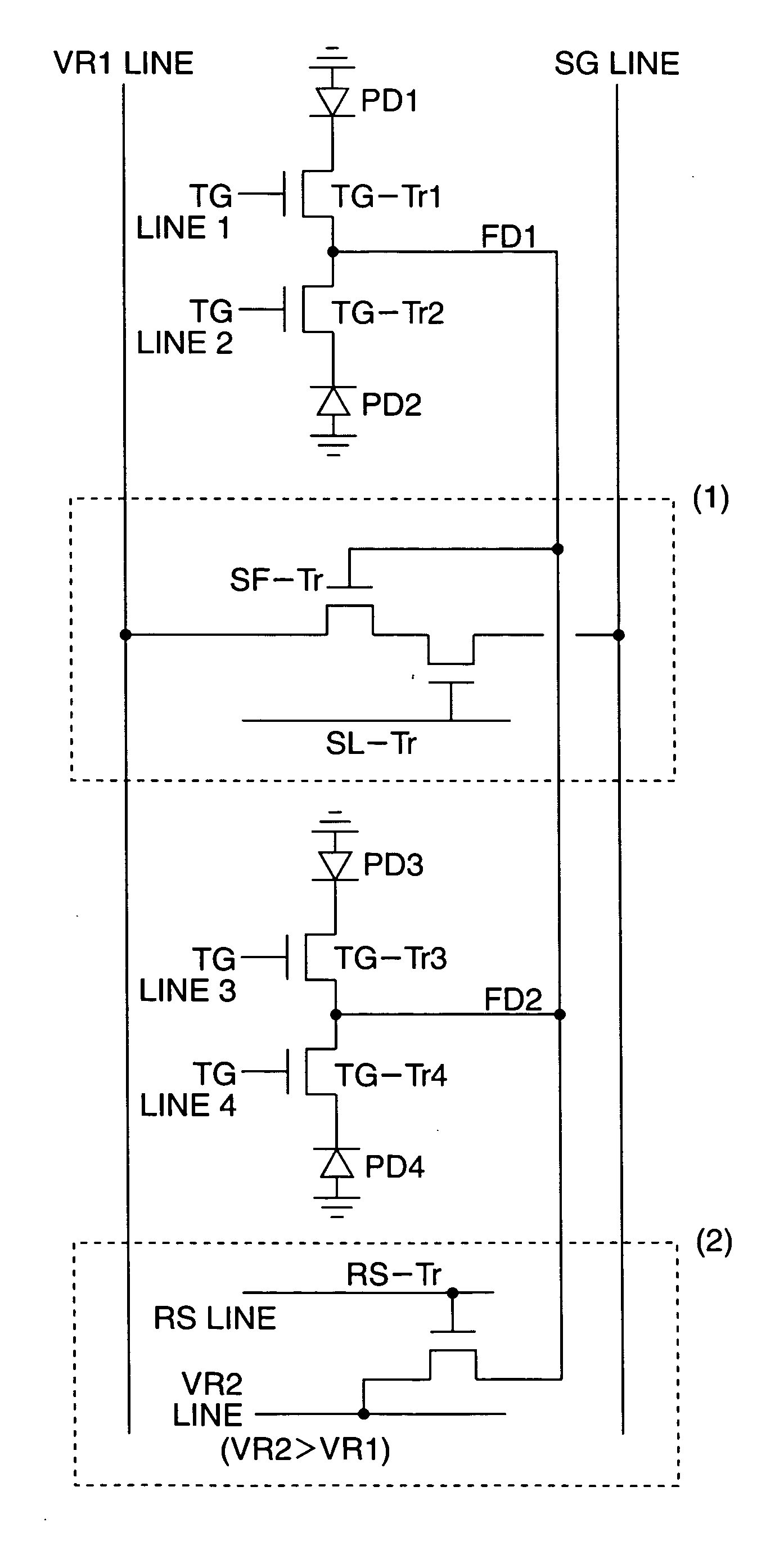
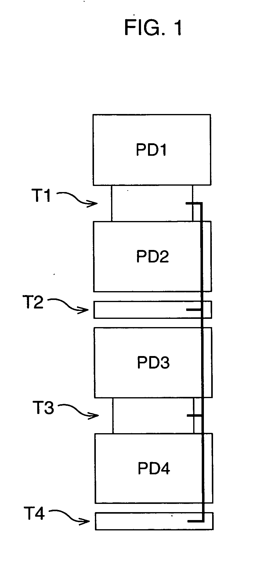
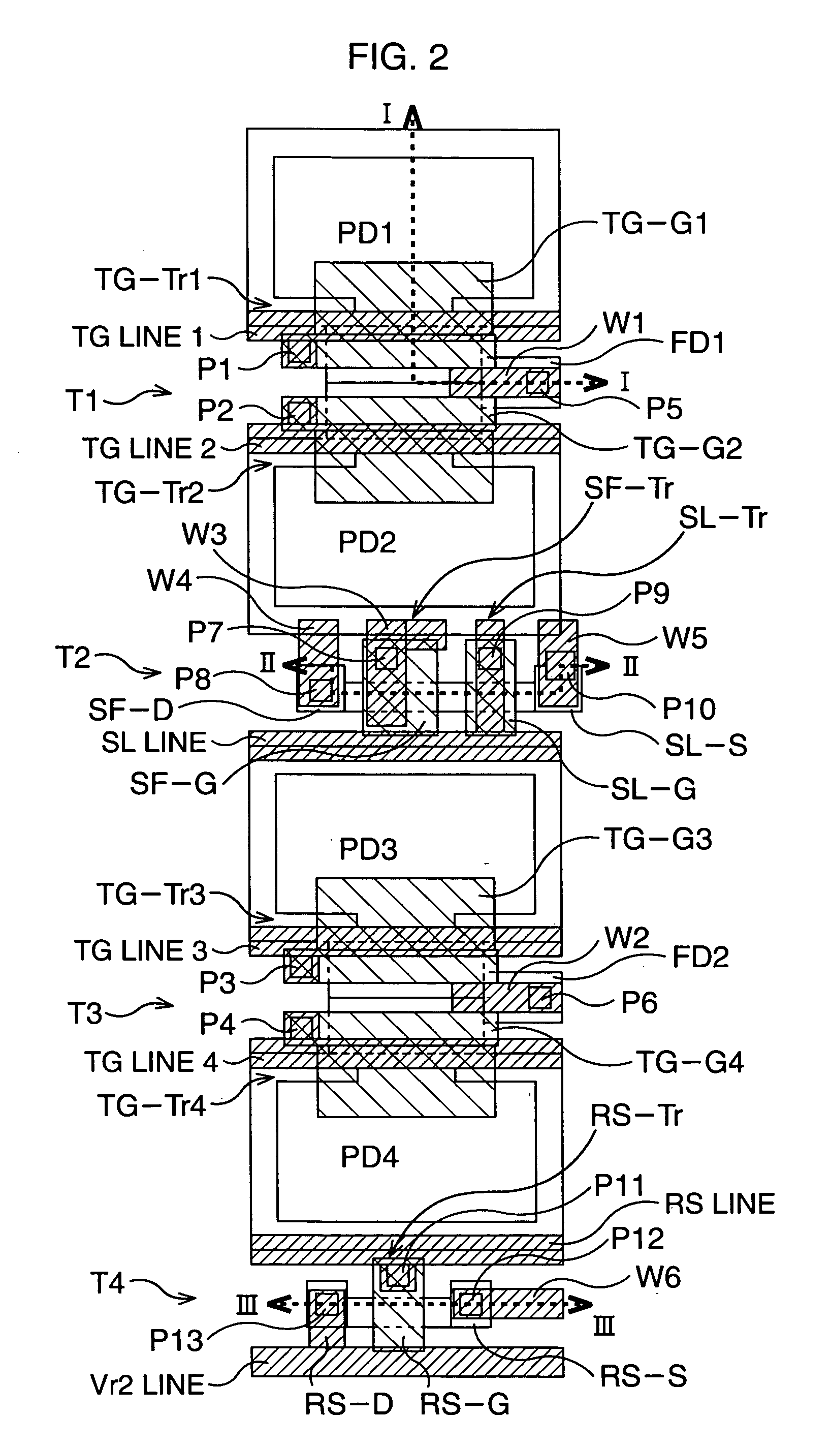
[0055]FIG. 1 is a schematic view illustrating the basic structure of the CMOS image sensor (a sensor unit including four PDs aligned along the column direction: simply referred to as a sensor unit hereafter) according to the first embodiment. FIG. 2 is a schematic plan view illustrating, in detail, the arrangement of the sensor unit of FIG. 1. FIG. 3 is a schematic view illustrating two sensor units, and FIG. 4 is a schematic plan view illustrating, in detail, the arrangement of four sensor units (inside of the dashed line corresponds to a single sensor unit). Here, FIGS. 2 and 4, illustrate, as the basic structure of the sensor unit, how a first level wiring layer is formed on the gate electrode of respective transistors.
[0056] As shown in FIGS. 1 and 2, the basic structure of the sensor unit of the present embodiment is composed of photodiodes PD1 to PD4 disposed in alignment along the column direction, a transistor structure ...
PUM
 Abstract
Description
Claims
Application Information