Organic light emitting display

a light-emitting display and organic technology, applied in the field of organic light-emitting displays, can solve the problems of insufficient time to charge the load inconvenient charging of the data line, and non-uniform illumination

Active Publication Date: 2008-06-26
SAMSUNG DISPLAY CO LTD
View PDF9 Cites 169 Cited by
  • Summary
  • Abstract
  • Description
  • Claims
  • Application Information

AI Technical Summary

Benefits of technology

[0021]Accordingly, an object of the present invention is to provide an organic light emitting display that can be suitable for a high quality and high resolution display by rapidly charging a data voltage using a voltage programming technique, after compensating for deviations, such as the threshold and mobility of the driving transistors, using a current programming technique.

Problems solved by technology

In the pixel circuit of the voltage programming technique discussed above, the luminance is non-uniform due to deviations in mobility and threshold voltage of a TFT caused by non-uniformities in the manufacturing process.
However, the current (IOLED) flowing to the OLED is a minute current, and the pixel circuit is controlled by the minute current (IDATA), so that it has a problem in that it takes a considerable amount of time to charge the data line.
Therefore, there is a problem in that there is not sufficient time to charge the load of the data line, considering a line time of several tens of μs.

Method used


Image

  • Organic light emitting display
  • Organic light emitting display
  • Organic light emitting display

Examples


Embodiment Construction

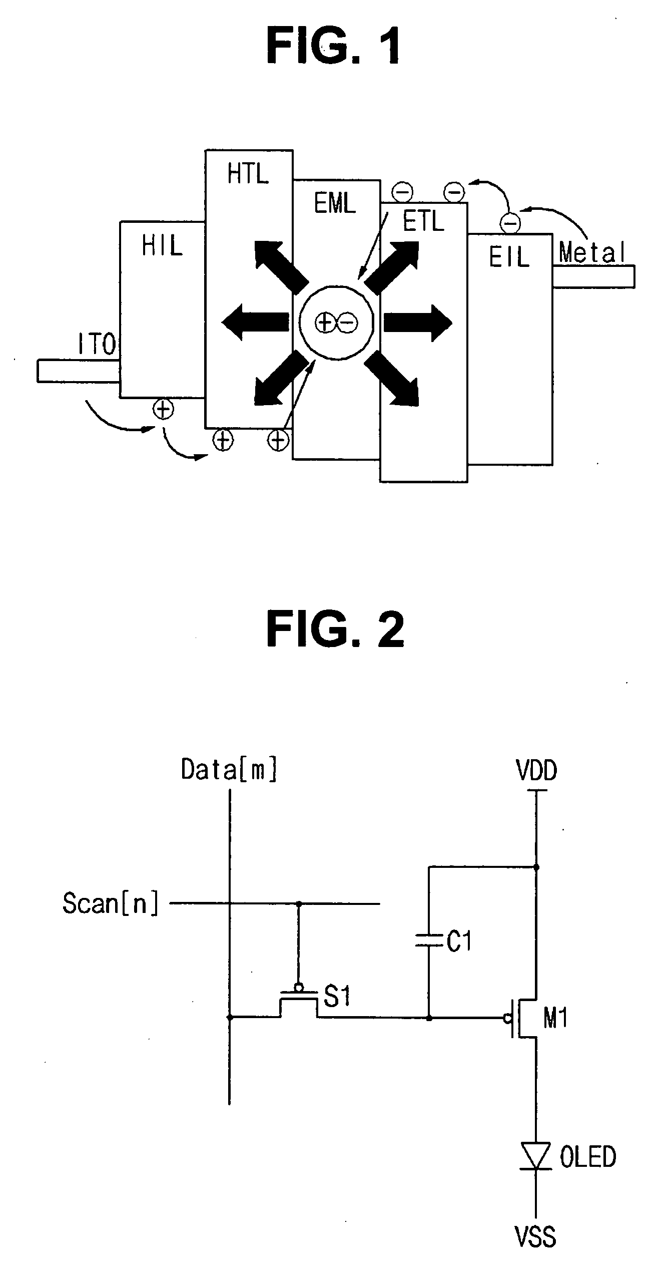
[0047]Hereinafter, exemplary embodiments of the present invention are described in detail with reference to the accompanying drawing. The aspects and features of the present invention and methods for achieving the aspects and features will be apparent by referring to the embodiments to be described in detail with reference to the accompanying drawings. However, the present invention is not limited to the embodiments disclosed hereinafter, but can be implemented in diverse forms. The matters defined in the description, such as the detailed construction and elements, are merely specific details provided to assist those of ordinary skill in the art in a comprehensive understanding of the present invention, and the present invention is only defined within the scope of the appended claims. In the entire description of the present invention, the same drawing reference numerals are used for the same elements across various figures.

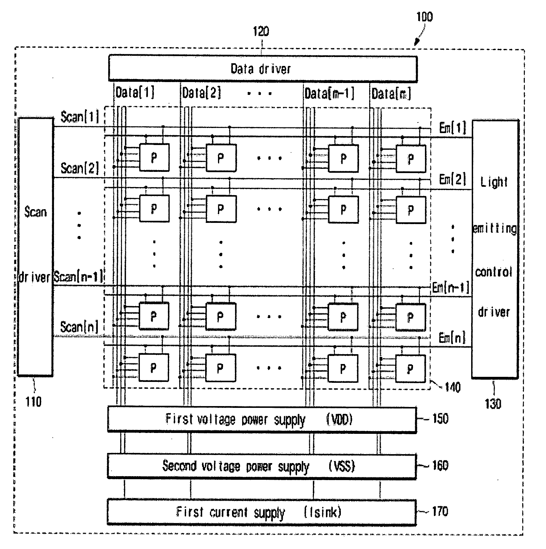
[0048]FIG. 4 is a block diagram of an organic light emittin...


PUM


Abstract

An organic light emitting display, suitable for a high quality and high resolution display device, rapidly charges a data voltage using a voltage programming technique, after compensating for a deviations in the threshold voltage and mobility of a driving transistor using a current programming technique. The organic light emitting display includes: a data line supplying a data signal; a scan line supplying a scan signal; a first switching element, electrically coupling its control electrode to the scan line, transferring the data signal supplied from the data line; a driving transistor, electrically coupling its control electrode to the first switching element, controlling a driving current of a first voltage line; a first capacitive element electrically coupled between the first switching element and the control electrode of the driving transistor; an Organic Light Emitting Diode (OLED), electrically coupled between the driving transistor and a second power voltage line, displaying an image by a current supplied from the driving transistor; and a fourth switching element compensating for deviations of characteristics of the driving transistor by supplying a current of the first current line to the driving transistor.

Description

CLAIM FOR PRIORITY[0001]This application makes reference to, incorporates the same herein, and claims all benefits accruing under 35 U.S.C.§119 from an application for ORGANIC LIGHT EMITTING DISPLAY earlier filed in the Korean Intellectual Property Office on 21 Dec. 2006 and there duly assigned Serial No. 10-2006-0131961.BACKGROUND OF THE INVENTION[0002]1. Field of the Invention[0003]The present invention relates to an organic light emitting display, and more particularly, the present invention relates to an organic light emitting display suitable for a high quality and high resolution display device, by rapidly charging a data voltage using a voltage programming technique, after compensating for deviations, such as a threshold voltage and a mobility of a driving transistor, using a current programming technique.[0004]2. Description of the Related Art[0005]Generally, a conventional organic light emitting display electrically excites a phosphor or a phosphorescent organic compound an...

Claims


Application Information

Patent Timeline
Patent Type & Authority Applications(United States)
IPC IPC(8): G09G3/32
CPCG09G3/3233G09G2300/0819G09G2310/0251G09G2300/0852G09G2300/0861G09G2300/0842G09G3/30G09G3/32G09G3/20H05B33/12
Inventor KIM, HYUNG-SOOLEE, WANG-JOCHUNG, BO-YONGCHOI, SANG-MOO
Owner SAMSUNG DISPLAY CO LTD
Why Eureka
Try Eureka