

Static random accee memory device
a memory device and random access technology, applied in the field of static random access memory devices, can solve the problems of difficult data write, difficult data write, and difficult to improve the two simultaneously, and achieve the effect of increasing the static margin in data read and data hold state, increasing the write margin, and lowering the electric potential of this nod
- Summary
- Abstract
- Description
- Claims
- Application Information
AI Technical Summary
Benefits of technology
Problems solved by technology
Method used
Image



Examples
first embodiment
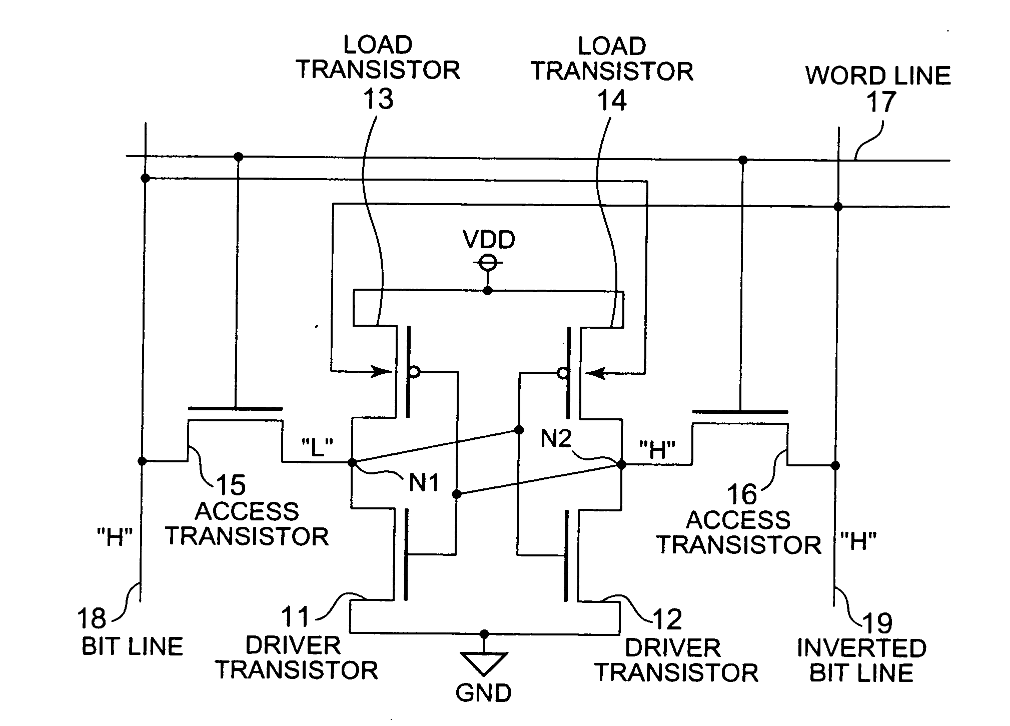
[0036]FIG. 1 is a circuit diagram of an SRAM cell according to a first embodiment of the present invention.
[0037]The SRAM cell shown in FIG. 1 has a pair of driver transistors ND1 and ND2, which are NMOS transistors, a pair of load transistors PL1 and PL2, which are PMOS transistors, and a pair of access transistors NA1 and NA2, which are NMOS transistors.
[0038]Source electrodes of the driver transistors ND1 and ND2 are both connected to a ground (GND). Source electrodes of the load transistors PL1 and PL2 are both connected to a power supply VDD. A drain electrode of the driver transistor ND1 is connected to a drain electrode of the load transistor PL1. This connection point will hereinafter be referred to as “node 1”. A drain electrode of the driver transistor ND2 is connected to a drain electrode of the load transistor PL2. This connection point will hereinafter be referred to as “node 2”. A gate electrode of the driver transistor ND1 and a gate electrode of the load transistor P...
embodiment 2
[0054]FIG. 6 is a structural diagram of a conventional dual port SRAM formed of eight transistors and capable of reading and writing data through each of the two ports.
[0055]FIG. 3 is a cell structural diagram for a modified version of the dual port SRAM of FIG. 6 to which the present invention is applied.
[0056]In the dual port SRAM, as in a single port SRAM (see FIG. 1), drains and gates of the two PMOS transistors P1 and P2 are connected to the node 1 and the node 2 such that the drain and gate of the transistor P1 are not connected to the same nodes that are connected to the drain and gate of the transistor P2, respectively. Sources of the transistors P1 and P2 are connected to the control signals S1 and S2. Stable operation is accomplished in the dual port SRAM by increasing the static noise margin in data read and in the data hold state and the write margin as in the single port SRAM.
[0057]When the present invention is applied to a dual port SRAM (WR+WR) formed of eight transis...
embodiment 3
[0058]A variation of the above-mentioned additional transistor control circuit for controlling the additional transistors will be described next. In the above embodiments, the control signals S1 and S2 are generated by adding the row select signal to the logic as well as the write enable signal, the column select signal, and the data input signal. By thus adding the row select signal to the logic as well as other signals, the control signals S1 and S2 can be controlled to be brought to the L level only when the node 1 or the node 2 shifts from the H level to the L level.
[0059]An effect substantially equal to the one that is obtained when the row select signal is added to the logic for controlling the control signals S1 and S2 can be obtained without adding the row select signal to the logic. In this case, the additional transistor control circuit which controls the control signals S1 and S2 can have a simpler structure and, moreover, SRAM cells that share a bit line can share the sa...
PUM
 Abstract
Description
Claims
Application Information