Semiconductor device

a technology of semiconductors and devices, applied in the direction of semiconductor devices, basic electric elements, electrical equipment, etc., can solve problems such as fluctuation of breakage voltage, and achieve the effect of suppressing the occurrence of electric field concentration and suppressing fluctuations of breakage voltag

Active Publication Date: 2015-05-07
SEIKO EPSON CORP
View PDF6 Cites 1 Cited by
  • Summary
  • Abstract
  • Description
  • Claims
  • Application Information

AI Technical Summary

Benefits of technology

This patent describes a semiconductor device with a diode that has less change in its breakdown voltage. This means that this device is more stable and reliable.

Problems solved by technology

The above-described diode is problematic in that the breakdown voltage fluctuates if the diode is repeatedly used.

Method used


Image

  • Semiconductor device
  • Semiconductor device
  • Semiconductor device

Examples


embodiment 1

[0033]FIGS. 1 and 2 are cross-sectional views illustrating a method for manufacturing a semiconductor device according to an aspect of the invention. FIG. 3 is a plan view of the semiconductor device shown in FIG. 2C.

[0034]As shown in FIG. 1A, a silicon substrate 11 is prepared. Next, as shown in FIG. 1B, an N-type buried layer 12 (also referred to as a “fourth impurity region”) is provided on the silicon substrate 11. Next, as shown in FIG. 1C, a P-type epitaxial growth layer 13 is provided on the N-type buried layer 12.

[0035]Next, as shown in FIG. 1D, in the P-type epitaxial growth layer 13, a cathode 14 composed of an N−-type impurity region (also referred to as a “first impurity region”) and N−-type third impurity regions 15 are provided. The cathode 14 and the third impurity regions 15 are located on the N-type buried layer 12, and they are electrically connected to the N-type buried layer 12. The N− type cathode 14 has a planar shape that is the shape of a rectangle whose corn...

embodiment 2

[0048]FIGS. 4 and 5 are cross-sectional views illustrating a method for manufacturing a semiconductor device according to an embodiment of the invention. FIG. 6 is a plan view of the semiconductor device shown in FIG. 5C.

[0049]The steps shown in FIGS. 4A to 4D are the same as those shown in FIGS. 1A to 1D.

[0050]Next, as shown in FIG. 5A, field insulating films 26, 27, 28 and 29 composed of trench oxide films are provided in the P-type epitaxial growth layer 13. The term “trench oxide film” used in this specification refers to an oxide film provided within a trench. For example, the field insulating films 26 and 29 may be shallow trench isolation (STI) films. The field insulating films 26, 27, 28 and 29 may be formed simultaneously.

[0051]An active region is provided on the inner sides of the field insulating films 27 and 28, and a cathode 14 is provided in the active region. First corner portions 27a, 27b, 28a and 28b are provided on the inner sides of the field insulating films 27 a...


PUM


Abstract

A semiconductor device including field insulating films and having first corner portions, provided on a P-type epitaxial growth layer; an N−-type cathode that is provided in the P-type epitaxial growth layer and is located on the inner sides of the field insulating films; and a P−-type anode that is formed on the cathode so as to be in contact with the cathode and covers the first corner portions provided on the inner sides of the field insulating films, wherein the junction between the cathode and the anode serves as a PN junction of the diode, and the PN junction is spaced apart from the first corner portions.

Description

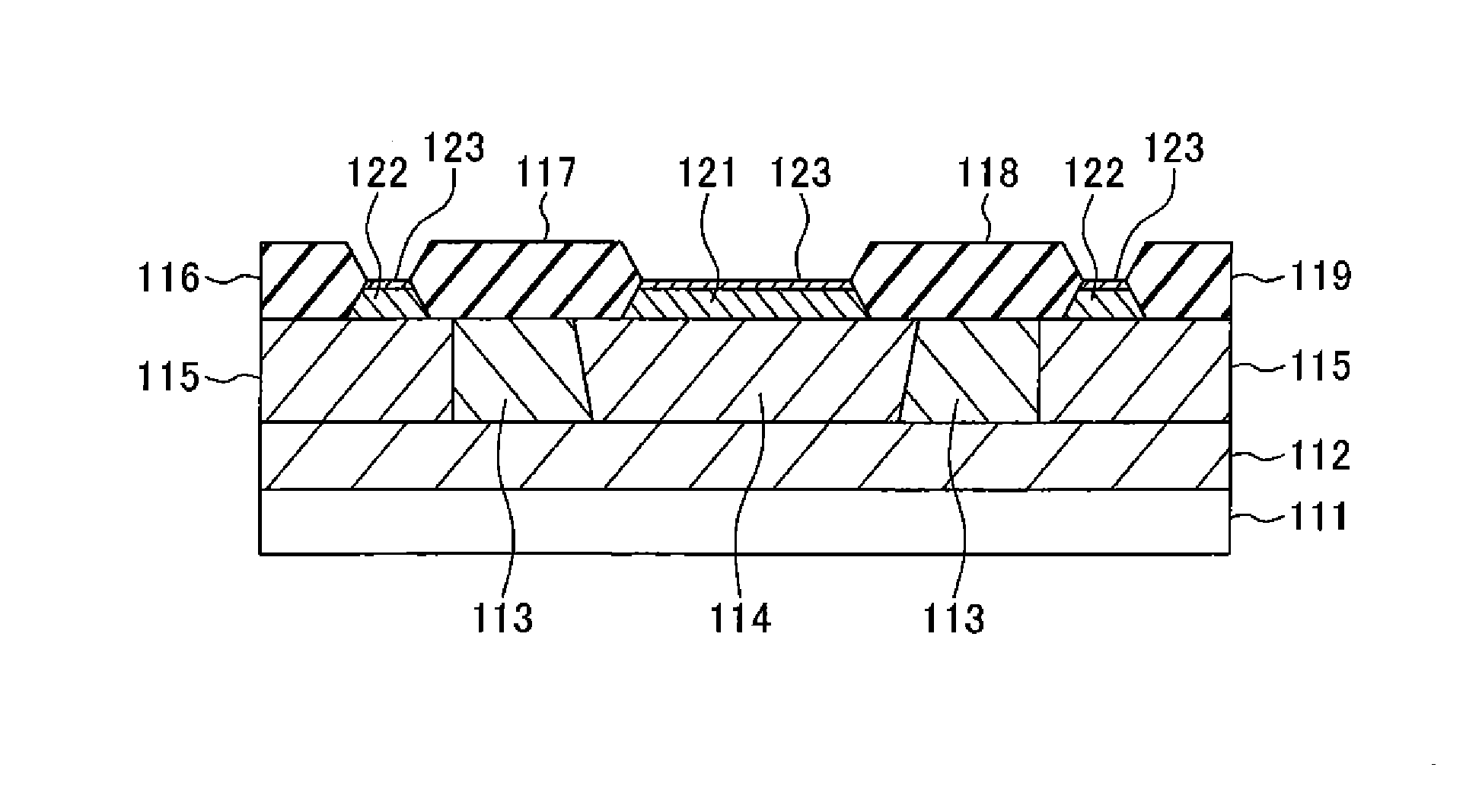
CROSS REFERENCE[0001]The entire disclosure of Japanese Patent Application No. 2013-229972, filed Nov. 6, 2013, is expressly incorporated by reference herein.BACKGROUND[0002]1. Technical Field[0003]The present invention relates to a semiconductor device including a diode.[0004]2. Related Art[0005]FIG. 7 is a cross-sectional view of a semiconductor device according to a related art. A vertical zener diode included in the semiconductor device is disclosed in US 2012 / 0074522 (FIG. 2).[0006]The semiconductor device shown in FIG. 7 includes a silicon substrate 111, and an N-type buried layer 112 provided on the silicon substrate 111. A P-type epitaxial growth layer 113 is provided on the N-type buried layer 112, and field insulating films 116, 117, 118 and 119 made of LOCOS oxide films are provided on the P-type epitaxial growth layer 113.[0007]A cathode 114 composed of an N−-type impurity region is provided in the P-type epitaxial growth layer 113 that is on the inner sides of the field ...

Claims


Application Information

Patent Timeline
Patent Type & AuthorityApplications(United States)
IPC IPC(8): H01L29/861H01L29/06
CPCH01L29/8611H01L29/0649H01L29/0619H01L29/06H01L29/0607H01L29/866H01L29/0615H01L29/66106
InventorSAKUMA, SHIGEYUKI
OwnerSEIKO EPSON CORP