

Phased array device and calibration method therefor
a phased array and calibration method technology, applied in the field of electronic circuits, can solve the problems of intra-chip variation inherent in the variation of the beam pattern, adversely affecting the beam pattern,
- Summary
- Abstract
- Description
- Claims
- Application Information
AI Technical Summary
Benefits of technology
Problems solved by technology
Method used
Image

Examples
Embodiment Construction
[0016]A detailed description is given in the following embodiments with reference to the accompanying drawings.
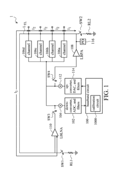
[0017]FIG. 1 is a block diagram of a phased-array device 1 (phased array device) according to an embodiment of the invention, comprising a baseband circuit 100, down-converter and filter 102, modulator 104, channel elements 106a-d, Loopback Power Amplifier (LBPA) 108, Loopback Low Noise Amplifier (LBLNA) 110, demodulator 112, up-converter and filter 114, power meter (PM) 116, switches SW1-SW4, resistors RL1 and RL2, and transmission line LTL.
[0018]The channel elements 106a-d can comprise transmitter front ends and / or receiver front ends. Each channel element may suffer from a channel-to-channel mismatch due to differences in circuit elements and connection routes in the transmitter front ends and / or receiver front ends. The channel elements 106a-d are connected in an equal distance 12 to one another by the transmission line LTL. The transmission line LTL connects all the ch...
PUM
 Abstract
Description
Claims
Application Information